ASML Spinout Invisix Raises €20M to See Inside the Chips Optics Can’t
Companies Mentioned
Why It Matters
Yield improvements at advanced nodes translate into billions of dollars, and Invisix’s non‑destructive inspection could become a critical tool for fabs racing to the next generation of chips.
Key Takeaways
- •Invisix raised €20M (~$22M) to develop soft‑x‑ray metrology.
- •Backed by Hitachi Ventures, imec.xpand and an undisclosed tier‑1 fab.
- •Targets hidden‑layer yield losses in 2 nm and beyond chips.
- •Uses high‑harmonic soft‑x‑ray laser and AI reconstruction.
Pulse Analysis
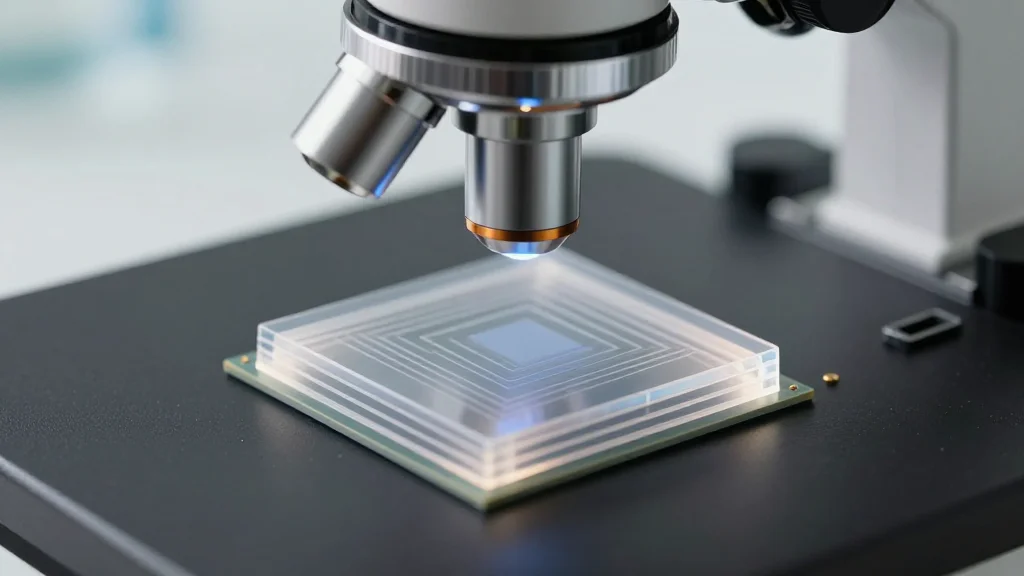
The semiconductor industry faces a paradox: as transistors shrink to a few nanometers and stack in three dimensions, traditional optical metrology can no longer see the critical features buried deep within the wafer. This blind spot drives costly, destructive testing methods that erode yields and slow time‑to‑market. Invisix’s approach leverages high‑harmonic generation to produce soft‑x‑ray pulses, a technique recognized by the 2023 Nobel Prize in Physics, enabling a richer three‑dimensional signal that can be reconstructed with machine‑learning algorithms. By delivering non‑invasive, high‑resolution imaging, the company promises to close the measurement gap that currently hampers advanced node production.
Beyond the technology, Invisix’s backing signals strong market validation. Hitachi Ventures, imec.xpand, Doosan and an unnamed tier‑1 fab—rumored to be Samsung—have committed capital, indicating that major players see immediate value in a tool that can directly improve yield. In a sector where a single percentage‑point increase in yield can add billions to profit margins, the financial incentives are compelling. The seed round’s oversubscription also reflects a broader European push to retain critical semiconductor capabilities, with the Netherlands and Belgium nurturing a deep‑tech ecosystem around ASML’s legacy.
The path to commercial success, however, remains steep. Transitioning from a laboratory demonstration to a production‑ready system requires scaling the laser source, integrating the reconstruction pipeline, and proving reliability in high‑volume fabs. If Invisix can deliver a turnkey solution that fits into existing fab workflows, it could become a cornerstone of next‑generation process control, reshaping how chipmakers manage yield and accelerating the rollout of 2 nm and sub‑2 nm technologies. The company’s progress will be closely watched by both investors and manufacturers eager for a competitive edge in the relentless race for smaller, faster chips.
ASML spinout Invisix raises €20M to see inside the chips optics can’t
Comments
Want to join the conversation?
Loading comments...