Accelerating Static ESD Simulation for Full-Chip and Multi-Die Designs with Synopsys PathFinder-SC
•February 17, 2026
0
Why It Matters
Early ESD verification prevents costly re‑spins and accelerates time‑to‑market for advanced‑node chips and chiplet architectures, where discharge failures are increasingly critical.
Key Takeaways
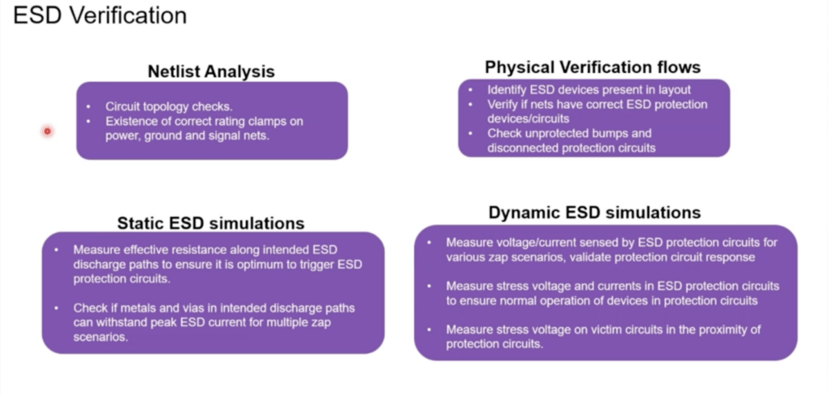
- •ESD verification consumes up to 50% engineering effort.
- •PathFinder‑SC simulates full‑chip ESD in hours, not days.
- •Supports multi‑die, 3D‑IC, and package‑level analysis.
- •Distributed Seascape engine scales to billions of nodes.
- •Early detection cuts redesign risk and time‑to‑market.
Pulse Analysis
Advanced packaging technologies such as chiplets and 3D‑ICs have amplified the electrostatic discharge (ESD) threat across the entire product lifecycle. Traditional RC‑only checks no longer capture the multiphysics interactions—inductance, thermal effects, and voltage‑drop—that can trigger latent failures. By moving ESD verification to the early physical‑design stage, engineers can evaluate discharge paths before tape‑out, dramatically reducing the debugging effort that historically consumes 30‑50% of design time.
PathFinder‑SC differentiates itself with a cell‑based modeling flow that extracts discharge circuits directly from layout databases (GDS, OASIS, DEF, LEF). Coupled with RedHawk‑SC’s certified extraction and electromigration engines, the platform delivers accurate effective‑resistance and current‑density metrics that align with foundry guidelines. Its Seascape distributed‑computing backbone parallelizes geometry processing, resistance extraction, and zap simulations across hundreds of cores, enabling full‑chip or multi‑die analyses involving millions of nodes to complete within a single workday. Multi‑scenario views further let designers explore variations in bump placement, clamp types, and extraction corners, providing a comprehensive risk picture from die to package.
The business impact is tangible: the webinar highlighted a 3D‑IC with 168 k protection diodes completing clamp‑to‑clamp checks in under 14 hours on 80 CPUs, and a 5 nm SoC finishing current‑density runs in 37 hours on 50 CPUs. Such speed translates into faster design sign‑off, lower silicon risk, and shortened time‑to‑revenue for high‑margin products. As the semiconductor industry pushes toward ever‑smaller nodes and heterogeneous integration, tools like PathFinder‑SC become essential for maintaining reliability while preserving competitive development cycles.
Accelerating Static ESD Simulation for Full-Chip and Multi-Die Designs with Synopsys PathFinder-SC
0
Comments
Want to join the conversation?
Loading comments...