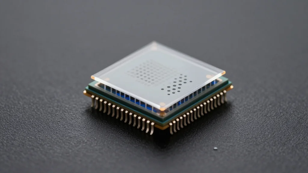
Dual-Gate Vertical Transistor Enables Stable Nanoscale 3D Chip Stacking
Key Takeaways
- •Dual-gate vertical transistor cuts off-state leakage to 10⁻¹² A.
- •Graphene top electrode enables fine channel control.
- •Low‑temperature, alignment‑free fabrication supports large‑area 3D stacking.
- •Micro‑hole lower electrode improves electric field penetration.
- •Enables high‑density, low‑power 3D semiconductor integration.
Pulse Analysis
The semiconductor industry is confronting the end of traditional Moore’s Law scaling, prompting engineers to explore three‑dimensional integration as a density‑boosting alternative. Conventional vertical transistors, however, suffer from uneven electric fields that cause leakage as channel lengths shrink, limiting their practical use. DGIST’s dual‑gate architecture tackles this head‑on by sandwiching the channel between a graphene drain gate and a patterned bottom gate, delivering uniform field penetration and suppressing off‑state currents to the picoampere range.
Beyond the electrical advantages, the process sidesteps costly alignment steps and runs at low temperatures, a rare combination that enables successive layer deposition without damaging existing structures. The micro‑hole pattern in the lower electrode acts as a conduit for the gate field, while a dedicated blocking layer eliminates parasitic leakage paths where electrodes overlap. This fabrication simplicity translates to large‑area, wafer‑scale production potential, a critical factor for commercial adoption of 3D stacking technologies.
The implications ripple across multiple market segments. High‑density logic and memory arrays can now be built with dramatically reduced footprint and power consumption, supporting the surge in edge‑AI and IoT devices. Moreover, the low‑temperature, flexible‑substrate compatibility opens doors for wearable and bendable electronics. As the industry seeks to extend performance gains without escalating costs, the dual‑gate vertical transistor positions itself as a cornerstone for the next generation of low‑power, ultra‑compact semiconductor solutions.
Dual-gate vertical transistor enables stable nanoscale 3D chip stacking
Comments
Want to join the conversation?