Eyeing the Massive HPC Opportunity for Unlocking Agentic AI with Silicon Photonics
•February 26, 2026
0
Why It Matters
By breaking copper’s bandwidth and power ceiling, silicon photonics can dramatically lower AI inference costs and accelerate the deployment of large‑scale agentic models. This shift positions hardware vendors and cloud providers to capture new market value in the AI‑driven HPC era.
Key Takeaways
- •Silicon photonics offers terabits per second bandwidth.
- •Latency can drop up to 90% versus copper.
- •Power per bit may halve with DWDM multiplexing.
- •Enables multi‑rack servers with thousands of GPUs.
- •Reduces AI token cost, boosting economic efficiency.
Pulse Analysis
The current HPC landscape is dominated by copper‑based interconnects such as Nvidia’s NVLink, which, despite being the fastest scale‑up solution today, is hitting physical limits in bandwidth, distance, and power consumption. As AI models grow larger and inference workloads demand ever‑higher data rates, the copper paradigm forces designers into costly cooling solutions and complex retimer architectures. This bottleneck is prompting the industry to explore optical alternatives that can sustain the data deluge without the thermal penalties of traditional metal wiring.
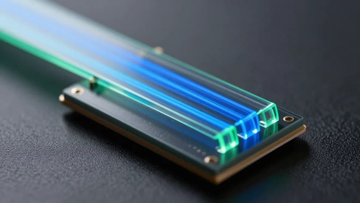
Silicon photonics, especially when combined with dense wavelength‑division multiplexing (DWDM), offers a compelling path forward. Scintil Photonics’ newly announced DWDM laser, fabricated on Tower Semiconductor’s line and integrated with TSMC’s COUPE platform, can deliver up to 3.2 Tbps per GPU while maintaining power consumption around 3.5 pJ/bit. The technology’s ability to multiplex up to 16 wavelengths on a single silicon strand translates into “bandwidth abundance,” allowing system architects to scale beyond the 100‑chip limit of today’s scale‑up servers and envision multi‑rack supercomputers with thousands of accelerators.
The business implications are profound. With latency reduced by up to 90% and a projected 50% cut in power per bit, operators can keep larger KV caches in memory, dramatically lowering the cost per token for generative AI services. Early adopters anticipate a two‑to‑three‑fold increase in utilization rates, effectively reducing AI compute expenses by a third. As major players signal deployment plans for 2028, silicon photonics is poised to become a cornerstone of the next wave of AI‑centric HPC infrastructure, reshaping vendor roadmaps and competitive dynamics across the cloud and data‑center markets.
Eyeing the Massive HPC Opportunity for Unlocking Agentic AI with Silicon Photonics
0
Comments
Want to join the conversation?
Loading comments...