How to Overcome the Advanced Node Physical Verification Bottleneck
Key Takeaways
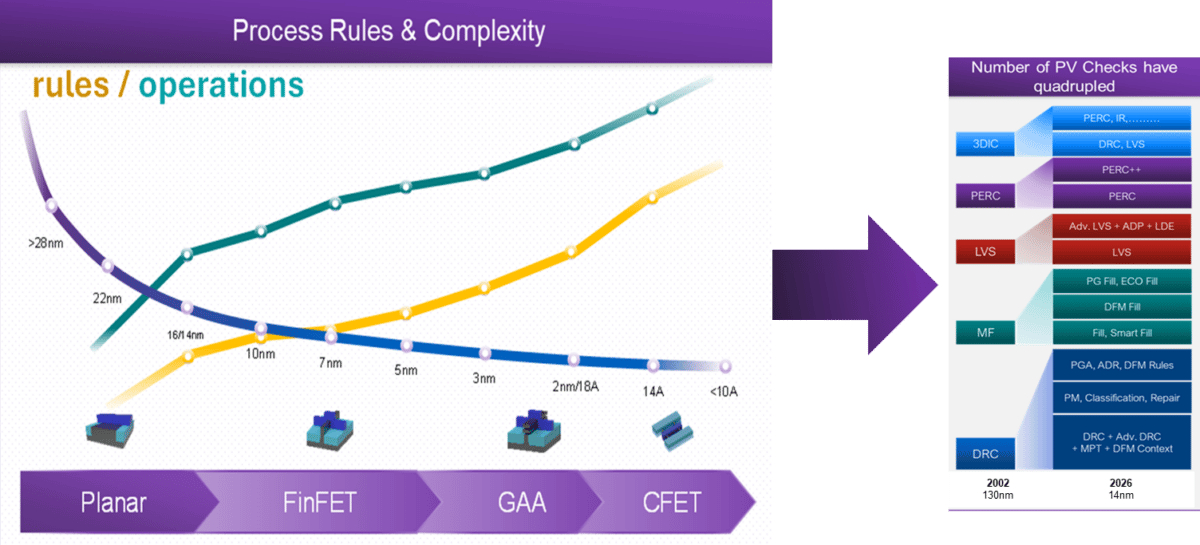
- •Physical verification checks have quadrupled at N2 nodes.
- •IC Validator cuts antenna check time 2‑4×, CPU use down 70%.
- •Elastic compute reduces verification cost by roughly 50%.
- •Integrated explorers enable fast DRC/LVS fixes within design environment.
- •Leading foundries certify IC Validator for advanced process nodes.
Pulse Analysis
Advanced semiconductor nodes such as N2 bring unprecedented rule density, with antenna, PERC ESD and other checks multiplying eightfold compared with earlier generations. Designers face full‑chip runs that can stretch from days to weeks, jeopardizing tape‑out schedules and inflating compute budgets. The industry’s traditional verification stacks, built for static, on‑premise workloads, simply cannot keep pace with the exponential growth in checks, prompting a search for more elastic, scalable solutions.
Synopsys IC Validator answers that need with its HyperSync architecture, which distributes verification tasks across thousands of CPU cores and dynamically scales to cloud or on‑premise clusters. By parallelizing antenna, DRC, LVS and PERC analyses, the platform delivers 2‑4× faster turn‑around while reducing core consumption by up to 70 %. The elastic compute model trims verification spend by roughly 50 % and eliminates queue bottlenecks, enabling designers to run full‑chip checks on demand rather than waiting for weeks. Tight integration with Fusion Compiler, 3DIC Compiler and StarRC creates a seamless sign‑off environment, allowing early‑exploration flows such as DRC Explorer and LVS Explorer to catch issues before they propagate.
The impact reaches beyond speed. Faster verification accelerates design closure, improves time‑to‑market, and lowers overall R&D expenditure—key competitive levers in a market where advanced‑node capacity is scarce. Foundry certifications across leading process nodes give customers confidence that the results meet production standards. As more chipmakers adopt chiplet‑centric, heterogeneous designs, tools that combine distributed processing with in‑design fix‑up will become indispensable, positioning IC Validator as a strategic asset for next‑generation silicon development.
How to Overcome the Advanced Node Physical Verification Bottleneck
Comments
Want to join the conversation?