(PR) NanoIC Launches Advanced Interconnect PDKs for Chip-to-Chip Designs
•March 2, 2026
0
Key Takeaways
- •NanoIC releases fine‑pitch RDL and D2W PDKs.
- •RDL achieves 1.3 µm lines, 20 µm microbump pitch.
- •Hybrid bonding removes copper bump parasitics, boosts bandwidth.
- •Early‑access kits target universities, start‑ups, SMEs.
- •Enables chiplet integration for AI, HPC, automotive.
Summary
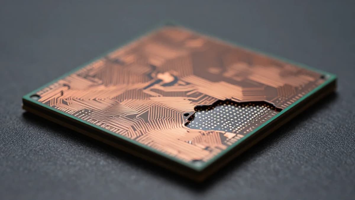
NanoIC, the imec‑coordinated European pilot line, announced the release of two advanced interconnect process design kits – a fine‑pitch redistribution layer (RDL) and a die‑to‑wafer (D2W) hybrid bonding kit. The RDL PDK supports line widths and spaces down to 1.3 µm and microbump pitches as tight as 20 µm, promising up to 40% faster communication and 15% lower energy per bit on UCIe‑Advanced interfaces. The D2W hybrid bonding kit replaces traditional copper bumps with oxide‑to‑oxide links, cutting parasitic losses and enabling ultra‑dense 3‑D chip‑to‑chip connections. These early‑access kits are aimed at universities, start‑ups and SMEs to accelerate chiplet‑based system development.
Pulse Analysis
The semiconductor ecosystem is rapidly shifting from monolithic dies to heterogeneous chiplet assemblies, and interconnect density has become the performance bottleneck. NanoIC’s fine‑pitch RDL PDK tackles this challenge by leveraging polymer‑based substrates that were previously limited to coarse routing. With line widths as narrow as 1.3 µm and microbump pitches of 20 µm, designers can achieve tighter signal paths, reducing latency and power consumption. This capability aligns with the UCIe‑Advanced specification, positioning European research labs to compete with leading foundries in high‑bandwidth, low‑energy packaging.
Equally transformative is the D2W hybrid bonding PDK, which replaces conventional copper microbumps with direct oxide‑to‑oxide connections. The elimination of copper‑induced parasitics yields cleaner signal integrity and higher bandwidth, crucial for AI accelerators and next‑generation GPUs that demand terabit‑per‑second inter‑chip links. By providing a validated design rule set and automated routing tools, the kit shortens the development cycle, allowing innovators to move from simulation to silicon faster than ever before.
Beyond the technical merits, the strategic impact of these early‑access kits cannot be overstated. They democratize cutting‑edge packaging technology, giving startups and academic groups the same design foundation previously reserved for large incumbents. This openness accelerates ecosystem growth, fuels talent development, and encourages a broader range of applications—from autonomous vehicle processors to edge‑AI modules. As the kits mature toward full tape‑out capability, they will likely become a cornerstone of Europe’s push to lead in beyond‑2 nm chiplet integration.
Comments
Want to join the conversation?