Siemens EDA Expands AI and Advanced Packaging Collaboration with TSMC
Key Takeaways
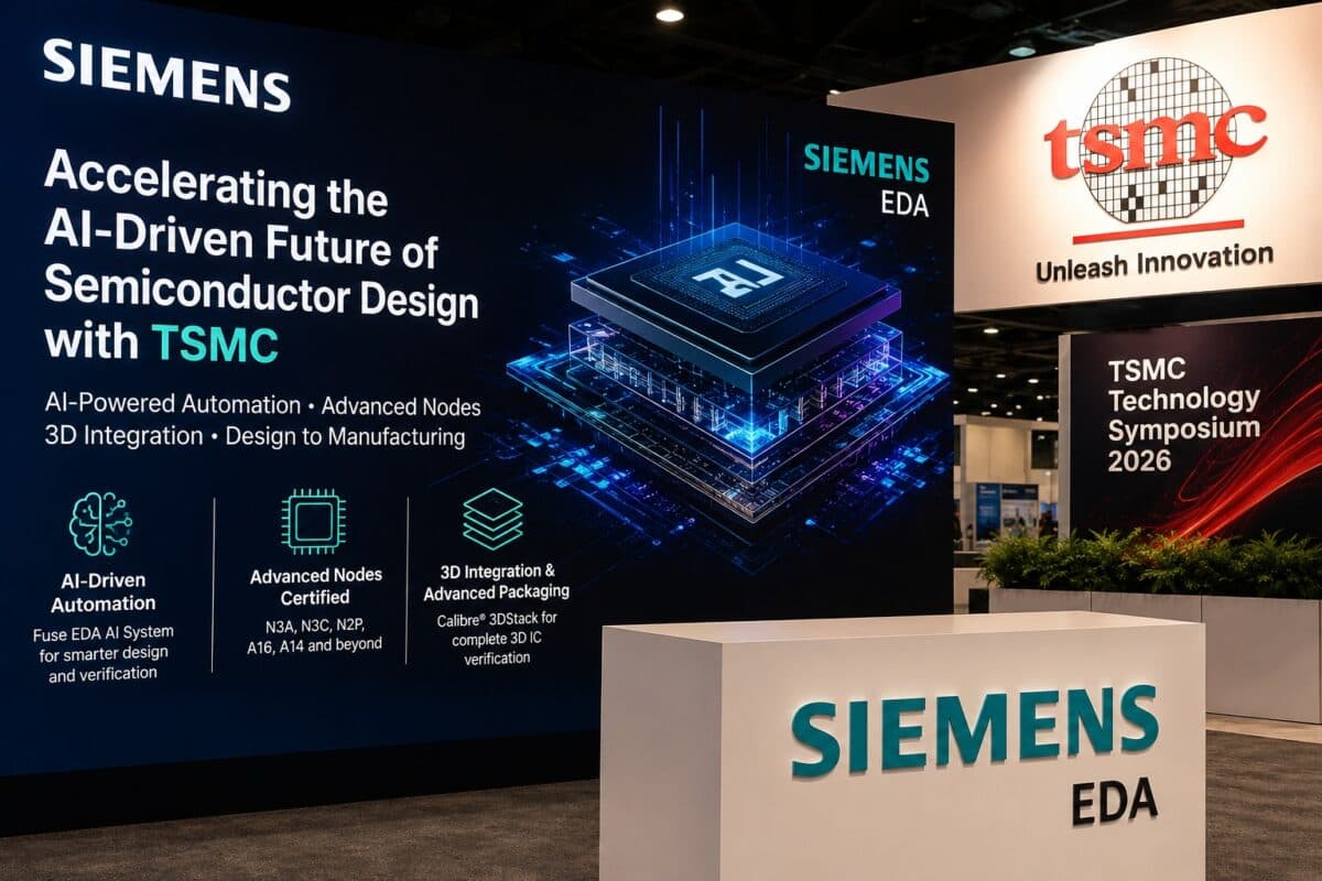
- •AI‑powered DRC fixing and verification integrated into Siemens’ Calibre suite
- •Siemens tools certified on TSMC N3A, N3C, N2P, A16, A14 nodes
- •Calibre 3DStack supports inter‑chiplet DRC and current density analysis
- •Fuse AI System provides autonomous design optimization for AI chips
- •Partnership deepens Siemens role in TSMC’s Open Innovation Platform
Pulse Analysis
The semiconductor industry is at a tipping point where AI workloads demand unprecedented design complexity. Traditional manual verification can no longer keep pace with the multi‑die, 3D‑stacked architectures powering high‑performance computing and automotive processors. AI‑enabled EDA tools are emerging as the solution, using machine learning to predict rule violations, suggest fixes, and streamline physical verification, thereby shrinking design cycles and reducing costly re‑spins.
At the 2026 TSMC Technology Symposium, Siemens EDA leveraged this trend by unveiling a suite of AI‑driven capabilities tailored for TSMC’s most advanced process technologies. The Fuse AI System now automates design rule check (DRC) remediation and offers intelligent optimization recommendations, while Calibre and Aprisa incorporate these insights directly into production workflows. Certification on nodes such as N3A, N3C, N2P, A16 and A14 ensures that customers can begin tape‑out on sub‑2 nm platforms with validated flows, mitigating risk on multi‑billion‑dollar investments. Additionally, Calibre 3DStack addresses the growing need for rigorous 3D packaging verification, covering inter‑chiplet connectivity, antenna effects, and current density analysis.
The partnership signals a broader shift in the EDA market, where vendors compete not just on tool performance but on AI orchestration and ecosystem integration. By embedding its AI suite within TSMC’s Open Innovation Platform, Siemens positions itself as a strategic bridge between design and manufacturing, offering a unified, automated path from concept to silicon. This alignment is likely to accelerate AI‑accelerator rollouts, enhance yield on advanced nodes, and set a new benchmark for productivity in an industry grappling with escalating design challenges.
Siemens EDA Expands AI and Advanced Packaging Collaboration with TSMC
Comments
Want to join the conversation?