SoC PLANNER: A New Generation of SoC Design Exploration Solution Managing Cost-Effectiveness and Sustainability
Key Takeaways
- •SoC PLANNER cuts exploration time by up to 75×
- •Automates RTL generation from Pareto‑optimal configurations
- •Introduces unique eco‑design footprint score for chips
- •Reduces design cycle time 30‑40% for low‑power AI subsystems
Pulse Analysis
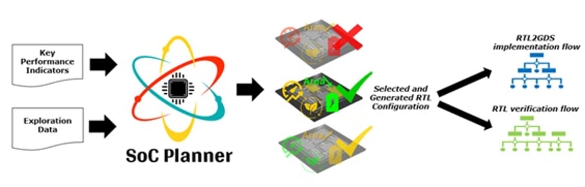
The semiconductor industry is confronting an unprecedented surge in design complexity, with more than a trillion chips produced annually and performance, power and area targets tightening across automotive, AI and high‑performance computing. Traditional manual exploration cannot keep pace, leading to longer time‑to‑market and higher engineering costs. SoC PLANNER tackles this bottleneck by unifying design‑space exploration, pre‑synthesis analysis and automatic RTL generation in a single, AI‑driven workflow. By feeding KPI ranges into its autonomous engine, the platform evaluates millions of configurations, ranks them on power, performance, area and a novel eco‑design footprint, then delivers synthesis‑ready RTL without human intervention.
Sustainability is becoming a decisive factor for chip manufacturers as regulatory pressure and corporate ESG goals intensify. The inclusion of an eco‑design footprint score differentiates SoC PLANNER from existing EDA tools, allowing architects to quantify the environmental impact of each configuration alongside traditional metrics. Early validation on a low‑power DNN accelerator (PNeuro) demonstrated a 30‑40% reduction in exploration time while preserving latency and energy efficiency, illustrating how sustainability can be baked into performance trade‑offs rather than treated as an afterthought.
For high‑performance computing, the platform’s speed gains are even more striking. An exhaustive manual search of hundreds of configurations would consume roughly 150 hours, whereas SoC PLANNER identified optimal solutions in under two hours—a 75× acceleration—while maintaining KPI accuracy. This dramatic productivity boost translates into lower R&D expenditures, faster silicon delivery and a stronger ability to iterate on next‑generation architectures. As chip nodes become more expensive and design windows shrink, tools like SoC PLANNER are poised to become essential components of modern semiconductor development pipelines.
SoC PLANNER: A New Generation of SoC Design Exploration Solution Managing Cost-effectiveness and Sustainability
Comments
Want to join the conversation?