What Is the 3nm Pessimism Wall and Why Is It An Economic Crisis?
Key Takeaways
- •3nm guard bands consume 25‑35% of clock period
- •Over‑design adds 2.5× buffer area and power
- •Recoverable margin can cut dynamic power 18‑20%
- •Reclaimed margin yields 300 MHz boost, millions revenue
- •SPICE‑accurate clock analysis eliminates pessimism wall
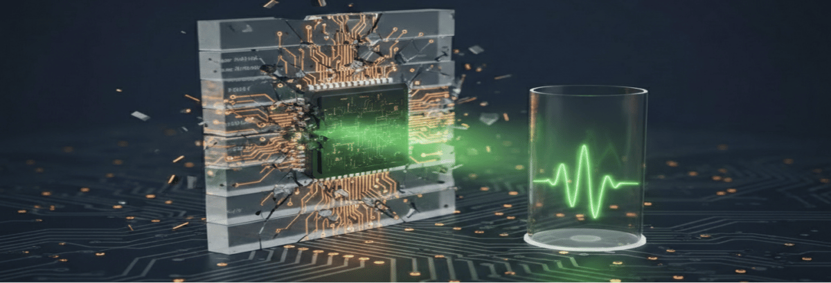
Pulse Analysis
The shift to 3 nm and beyond has exposed a hidden cost in semiconductor design: the Pessimism Wall. While foundries tout dramatic power‑performance‑area (PPA) improvements, most design teams still rely on legacy abstraction‑based sign‑off flows. These methods stack independent worst‑case assumptions—voltage sensitivity, jitter, aging—resulting in guard bands that consume up to a third of the clock period. The consequence is an over‑engineered clock network that inflates area, power, and time‑to‑market, turning theoretical node benefits into a performance mirage.
Economically, the impact is stark. A recoverable 10‑15% margin translates into an 18‑20% reduction in dynamic clock power, a critical factor when clock distribution accounts for 30‑40% of SoC consumption. Moreover, reclaiming that margin can add roughly 300 MHz to a 3 GHz target, shifting a sizable portion of production into premium performance bins and generating hundreds of millions in incremental revenue. The inflated area from over‑design also raises per‑die costs, eroding profit margins across high‑volume chips. In short, the Pessimism Wall is not a technical curiosity—it is a direct drain on profitability and market competitiveness.
The remedy lies in replacing abstraction with physics‑level analysis. Modern SPICE‑accurate engines, exemplified by ClockEdge’s Veridian suite, can simulate entire clock trees overnight, enforcing Kirchhoff’s laws across billions of transistors. This eliminates the need for conservative guard bands, uncovers hidden failure modes, and enables path‑specific aging assessments. By aligning modeling fidelity with the physical reality of 3 nm silicon, companies can safely reclaim margin, boost performance, and protect revenue streams, turning the Pessimism Wall from a crisis into a competitive advantage.
What is the 3nm Pessimism Wall and Why is it An Economic Crisis?
Comments
Want to join the conversation?