AlixLabs and VDL ETG Projects Announce MoU for Industrialization of APS Patterning
Why It Matters
Industrializing APS could lower semiconductor manufacturing costs and accelerate the transition to finer nodes, addressing a critical bottleneck in the industry’s scaling roadmap.
Key Takeaways
- •AlixLabs partners with VDL ETG to scale APS patterning tools
- •APS offers atomic layer etching, reducing reliance on EUV lithography
- •Collaboration targets batch manufacturing and turnkey semiconductor production lines
- •Industrialization aims to cut costs and speed up chip fabrication
- •VDL ETG brings system integration expertise to AlixLabs’ R&D
Pulse Analysis
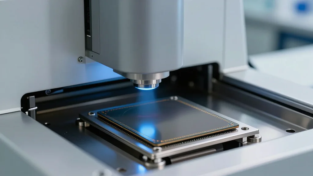
The semiconductor sector is confronting a convergence of cost pressure and physical limits as it pushes toward sub‑5‑nanometer nodes. Traditional multi‑patterning and extreme‑ultraviolet (EUV) lithography, while effective, demand ever‑higher capital expenditures and energy consumption. Atomic Pitch Splitting (APS) introduces a fundamentally different approach: by leveraging atomic‑layer etching, it can precisely split line pitches without the need for multiple exposure steps, promising a more sustainable and financially viable path for advanced patterning.
AlixLabs, a spin‑out from Lund University, has been refining APS since 2019, positioning the technology as a bridge between research labs and high‑volume fabs. The MoU with VDL ETG Projects, a Dutch engineering firm known for scaling complex equipment, is a strategic move to translate this R&D breakthrough into manufacturable hardware. VDL ETG’s capabilities in system integration, design for manufacturability, and turnkey line construction will accelerate the transition from prototype to batch production, ensuring that the APS tools meet the reliability and throughput standards required by leading foundries.
If successfully industrialized, APS could reshape the economics of next‑generation chip production. By reducing the number of lithography steps, fabs can lower per‑wafer cycle times and cut energy usage, directly impacting operating margins. Moreover, the technology aligns with the industry’s sustainability goals, offering a greener alternative to energy‑intensive EUV processes. Competitors will likely monitor the rollout closely, as early adopters stand to gain a competitive edge in cost‑sensitive markets such as mobile and IoT devices. The collaboration signals a broader trend of niche innovators partnering with established manufacturers to fast‑track disruptive semiconductor solutions.
AlixLabs and VDL ETG Projects announce MoU for industrialization of APS patterning
Comments
Want to join the conversation?
Loading comments...