AMD’s K6-III ‘Sharptooth’ Debuted This Week in 1999 with On-Die L2 Cache to Savage the Intel Pentium II — It Also Held the Line Against the Pentium III
•March 1, 2026
0
Why It Matters
The K6‑III demonstrated that on‑die cache could deliver competitive performance at lower cost, forcing Intel to accelerate its own cache innovations and shaping the CPU price‑performance curve of the early 2000s.
Key Takeaways
- •On‑die L2 cache gave K6‑III a performance edge
- •Extended Super Socket 7’s relevance beyond Intel’s Slot 1
- •Provided strong price‑performance versus early Pentium III
- •Bridged transition to Athlon K7 for mainstream users
- •Now a prized platform for retro‑computing enthusiasts
Pulse Analysis
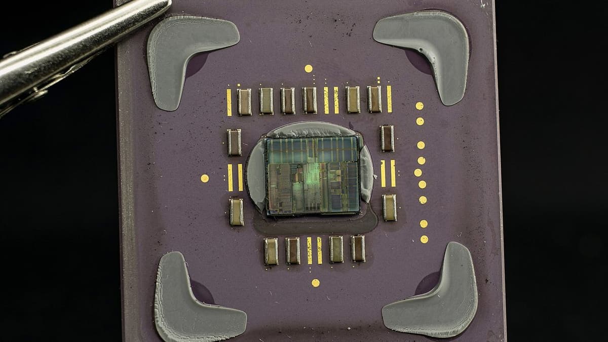
The debut of AMD’s K6‑III marked a pivotal moment in late‑1990s microprocessor design. By integrating a 256 KB L2 cache directly onto the silicon die, AMD broke the prevailing paradigm of external cache chips, reducing latency and boosting throughput for memory‑intensive workloads. This architectural leap allowed the K6‑III to outpace Intel’s Pentium II 450 MHz and hold its own against the freshly launched Pentium III, reshaping the competitive dynamics of the desktop market and reinforcing AMD’s reputation for innovative, cost‑effective solutions.
Beyond raw performance, the K6‑III’s launch extended the viability of the Super Socket 7 ecosystem. While Intel migrated to Slot 1 and later to the faster front‑side bus of the Pentium III, AMD’s commitment to an open, inexpensive socket gave system builders and upgraders a flexible upgrade path. Motherboards supporting 100 MHz FSB, AGP, and a range of memory types kept the platform relevant for several years, allowing users to extract additional value from existing hardware and smoothing the transition to the newer Athlon K7 architecture.
Today, the K6‑III enjoys a niche renaissance among retro enthusiasts. Its compatibility with a broad spectrum of legacy CPUs and GPUs, combined with excellent DOS performance, makes Super Socket 7 boards a popular foundation for vintage gaming and software preservation. The processor’s historical significance—demonstrating the power of on‑die cache and influencing Intel’s subsequent designs—continues to be studied by hardware historians, underscoring how a single architectural decision can ripple through an entire industry.
AMD’s K6-III ‘Sharptooth’ debuted this week in 1999 with on-die L2 cache to savage the Intel Pentium II — it also held the line against the Pentium III
0
Comments
Want to join the conversation?
Loading comments...