As Chips Go Vertical, Metrology Struggles to Keep Up
Companies Mentioned
Why It Matters
Without accurate, high‑throughput inspection of 3D structures, yield losses and power inefficiencies will rise, threatening the economics of advanced‑node chips and AI data‑center scaling.
Key Takeaways
- •Advanced nodes move scaling from X‑Y to Z‑axis, creating deep 3D structures
- •Conventional optical metrology and CD‑SEM cannot fully inspect buried sidewalls
- •TEM offers detail but is destructive and too slow for statistical control
- •Nearfield Instruments' AFM‑based QUADRA probes 15 nm openings with >100:1 aspect ratio
- •Inline, non‑destructive metrology is vital for yield, power efficiency, AI workloads
Pulse Analysis
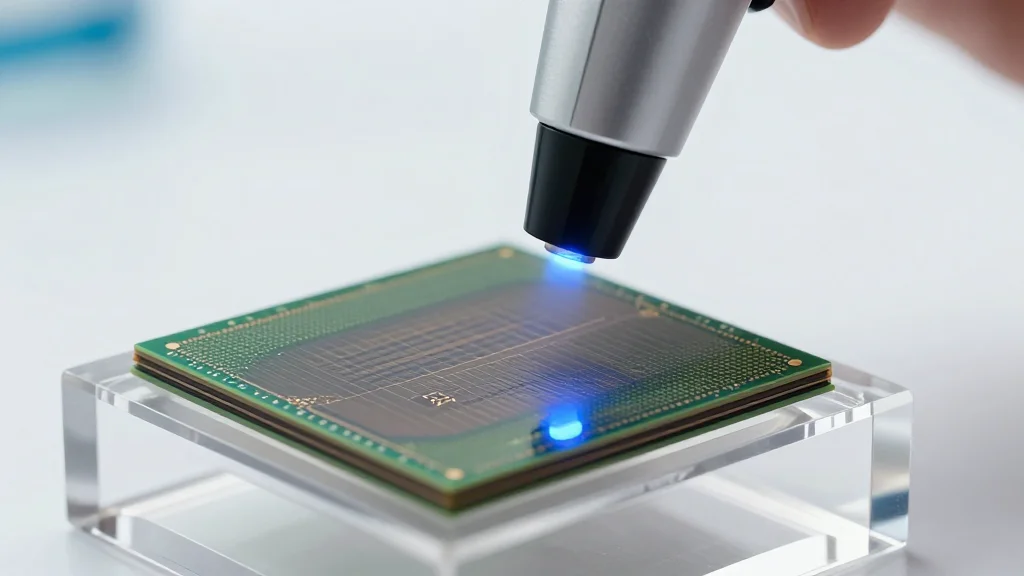
The migration toward gate‑all‑around transistors, stacked NAND, and hybrid‑bonded packages has turned semiconductor manufacturing into a three‑dimensional challenge. As critical features are etched deeper, variability no longer resides solely on the wafer surface but along buried sidewalls and internal interfaces. Conventional metrology—optical scatterometry and CD‑SEM—was optimized for planar geometries, leaving a blind spot that hampers process control and drives yield uncertainty. Meanwhile, transmission electron microscopy, though precise, requires wafer slicing and offers only localized snapshots, making it impractical for the high‑volume, statistical monitoring demanded by angstrom‑scale production.
To bridge this visibility gap, the industry is reviving atomic force microscopy (AFM) with a focus on speed and integration. Nearfield Instruments’ QUADRA platform exemplifies this trend, employing ultra‑narrow, torsion‑sensitive probes capable of entering trenches as small as 15 nm and delivering aspect‑ratio measurements exceeding 100:1. By capturing sidewall roughness and profile data inline, QUADRA promises TEM‑level structural insight without destroying wafers, enabling real‑time feedback loops that can tighten process windows and reduce the number of wafers sacrificed for failure analysis. The technology’s ability to generate full‑volume images rather than isolated cross‑sections marks a paradigm shift in how fabs visualize complex 3D devices.
The broader implication is that metrology is evolving from a peripheral quality‑check step into a strategic enabler of chip performance and energy efficiency. Precise sidewall control directly influences transistor leakage and switching voltage, which scales to substantial power savings across millions of chips in AI data centers. As manufacturers adopt hybrid metrology stacks—combining optical, e‑beam, X‑ray, and advanced AFM tools—the industry can achieve comprehensive, statistical visibility essential for sustaining Moore’s Law in the vertical dimension. This integrated approach not only safeguards yield but also accelerates the rollout of next‑generation nodes, reinforcing the competitive edge of firms that master 3D inspection.
As Chips Go Vertical, Metrology Struggles to Keep Up
Comments
Want to join the conversation?
Loading comments...