ASML Plans to Expand Beyond Chip Lithography Into Advanced Packaging
•March 2, 2026
0
Why It Matters
Advanced packaging is becoming a critical growth frontier for AI‑driven silicon, and ASML’s entry could create new revenue streams while tightening its role in the semiconductor supply chain.
Key Takeaways
- •ASML targeting advanced packaging market for AI chips.
- •Study phase spans 10‑15 years for new equipment.
- •Exploring larger chip printing beyond current EUV limits.
- •AI integration aims to accelerate machine control and QC.
- •Diversification could boost revenue beyond lithography.
Pulse Analysis
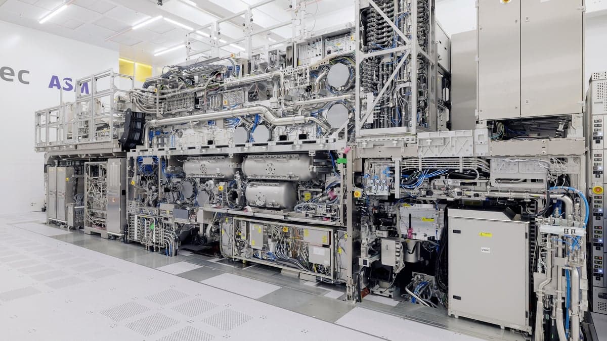
ASML has built an almost monopoly around extreme ultraviolet (EUV) lithography, the workhorse behind the most advanced logic nodes. As AI workloads drive demand for ever‑more complex silicon, chipmakers are turning to advanced packaging—stacking chiplets, integrating high‑bandwidth memory, and creating heterogeneous systems—to squeeze performance without shrinking transistors further. This shift is reshaping the semiconductor value chain, turning the back‑end of manufacturing into a growth engine. Companies like TSMC already leverage packaging to deliver Nvidia’s latest AI processors, signaling a market ripe for new equipment suppliers.
Against that backdrop, ASML announced a long‑term research agenda that looks ten to fifteen years ahead, aiming to design machines capable of handling the precise alignment, bonding, and thermal management required for chiplet stacking. The Dutch firm is also probing whether its optical systems can print larger die footprints, potentially bypassing current size constraints. Parallel to hardware development, ASML plans to embed artificial‑intelligence algorithms into the control software that drives its scanners, promising faster setup times, tighter process windows, and more reliable defect detection during wafer fabrication.
If successful, the move could diversify ASML’s revenue beyond lithography, which already accounts for the bulk of its earnings. By entering the advanced packaging arena, the company would position itself as a one‑stop shop for both front‑end patterning and back‑end integration, tightening its grip on the semiconductor supply chain. Competitors in the equipment space—such as Applied Materials and Lam Research—may feel pressure to accelerate their own packaging roadmaps, while chip designers could benefit from a more coordinated ecosystem. Ultimately, ASML’s expansion underscores how AI‑driven demand is blurring traditional boundaries between design, fabrication, and assembly.
ASML plans to expand beyond chip lithography into advanced packaging
0
Comments
Want to join the conversation?
Loading comments...