Chinese Startup Claims Photonic Chip Production without DUV Lithography, Says Nanoimprint Process Cuts Costs by 90% — 8-Inch Wafers Produced without Conventional Optical Lithography
Why It Matters
If the NIL process scales, it could lower China’s dependence on restricted DUV/EUV tools and dramatically cut production costs for photonic components, accelerating domestic data‑center and communications hardware.
Key Takeaways
- •Prinano’s NIL cuts photonic chip costs by ~90%
- •8‑inch wafers produced without any DUV lithography
- •Process targets waveguides, gratings, resonators—not high‑end CPUs
- •China seeks lithography alternatives amid ASML export bans
- •Yield and defect data remain undisclosed, raising commercial viability questions
Pulse Analysis
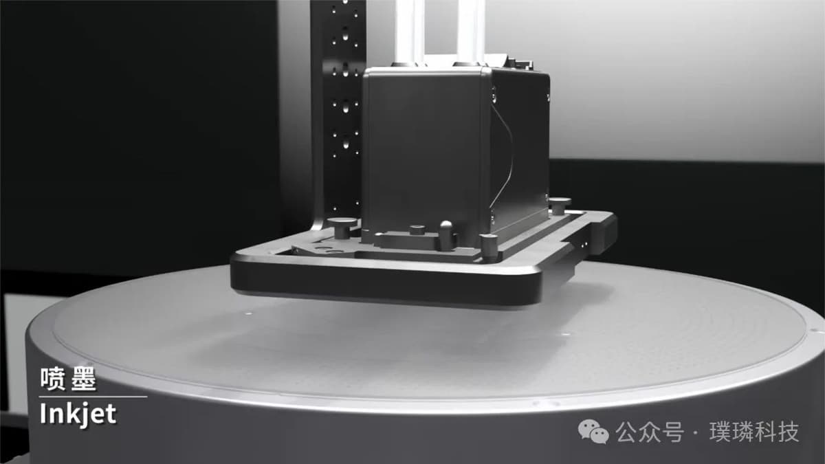
Traditional semiconductor manufacturing relies on deep‑ultraviolet (DUV) and extreme‑ultraviolet (EUV) lithography machines that cost hundreds of millions of dollars and are sourced almost exclusively from ASML. Export controls imposed by the United States have tightened China’s access to these tools, prompting a search for cheaper, domestically‑controlled alternatives. Nanoimprint lithography (NIL) sidesteps the complex optics of DUV/EUV by physically stamping nanoscale patterns onto a resist‑coated wafer, offering sub‑10‑nanometer resolution with a fraction of the capital expense. Prinano’s PL‑AS vacuum air‑cushion NIL system builds on this principle, adding wafer‑level pressure control and custom imprint materials to improve uniformity and feature fidelity.
Photonic chips, which manipulate light for high‑speed data transmission, sensing and LiDAR, are a natural fit for NIL because their structures—waveguides, gratings and ring resonators—repeat across the wafer and tolerate slightly higher defect densities than logic transistors. By delivering 8‑inch photonic wafers at roughly ten percent of DUV costs, Prinano could make optical interconnects more affordable for Chinese data‑center operators and telecom providers, narrowing the performance gap with Western suppliers. The cost advantage also opens opportunities for niche markets such as autonomous‑vehicle LiDAR and industrial sensing, where volume requirements are lower but price sensitivity remains high.
Despite the promising economics, the commercial viability of Prinano’s approach remains uncertain. The company has not disclosed production volumes, yield rates, or defect densities—metrics that determine whether NIL can meet the reliability standards of high‑volume manufacturing. Industry observers also caution that scaling NIL to larger 12‑inch wafers, required for mainstream logic chips, poses significant challenges in throughput and template wear. Nonetheless, the announcement signals a strategic shift: Chinese firms are increasingly willing to invest in non‑traditional lithography pathways to mitigate geopolitical risk. If yield improvements materialize, NIL could become a complementary process for specialized semiconductor segments, reshaping parts of the global supply chain and reducing reliance on ASML’s monopoly.
Chinese startup claims photonic chip production without DUV lithography, says nanoimprint process cuts costs by 90% — 8-inch wafers produced without conventional optical lithography
Comments
Want to join the conversation?
Loading comments...