D-Mode GaN Bidirectional Switches Reshape Power Conversion Topologies
Companies Mentioned
Why It Matters
By cutting parts and parasitics, the GaN BDS boosts converter efficiency and allows more compact, reliable designs, accelerating adoption of bidirectional power flow in EV, solar and data‑center markets.
Key Takeaways
- •Renesas' TP65B110HRU offers 650 V, 110 mΩ GaN bidirectional switching.
- •Single‑device BDS replaces back‑to‑back MOSFETs, cutting component count.
- •Lower on‑resistance and zero Qrr enable higher switching frequencies.
- •Enables compact topologies like totem‑pole PFC and single‑stage converters.
- •Challenges remain in scaling above 650 V and EMI management.
Pulse Analysis
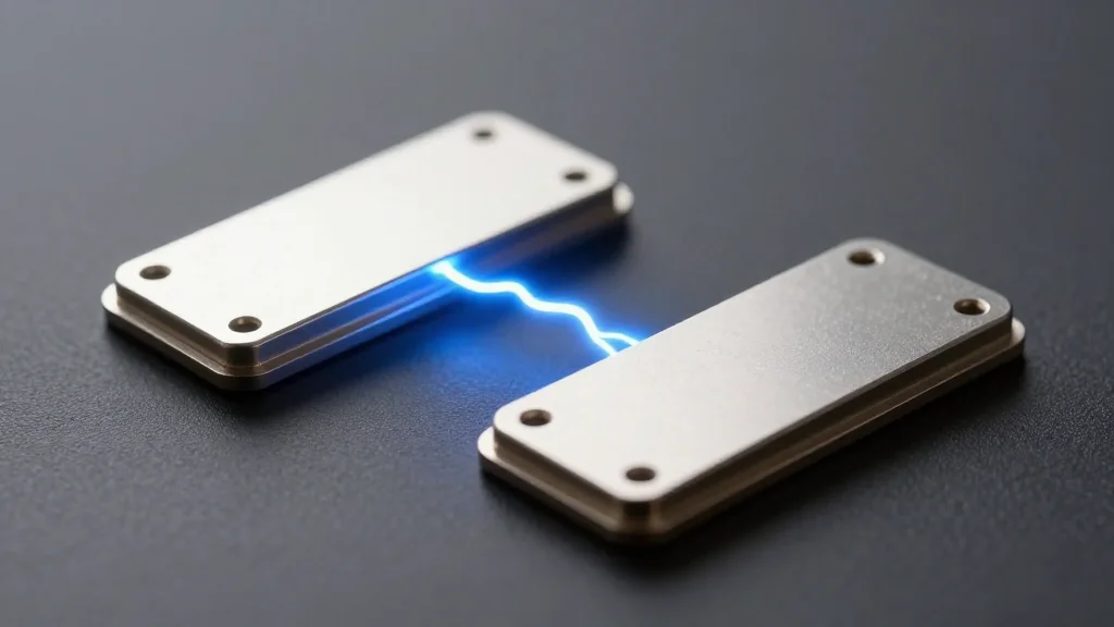
The emergence of depletion‑mode GaN bidirectional switches marks a shift from discrete back‑to‑back transistor arrangements to a single‑chip solution. By embedding two low‑voltage MOSFETs alongside a GaN channel, Renesas’ TP65B110HRU delivers true four‑quadrant operation while maintaining low on‑resistance and virtually zero reverse‑recovery charge. This architecture simplifies gate‑drive requirements, reduces stray inductance, and leverages GaN’s fast switching speeds, delivering efficiency gains that are difficult to achieve with traditional silicon devices.
System designers can now rethink converter topologies across multiple markets. In electric‑vehicle onboard chargers, the BDS enables seamless grid‑to‑vehicle and vehicle‑to‑grid power flow without extra free‑wheeling diodes, shrinking the charger footprint. Photovoltaic micro‑inverters benefit from reduced component count and higher switching frequencies, leading to lighter magnetics and better thermal performance. Data‑center power supplies can incorporate bidirectional capability to return stored energy to the grid during peak pricing, improving overall site‑level efficiency and resilience.
Despite the promise, adoption hinges on overcoming scalability and ecosystem hurdles. Extending the device class beyond the current 650 V rating to 1,200 V will require advanced substrate engineering and robust thermal solutions. Designers also need mature simulation models, reference designs, and clear EMI mitigation strategies to confidence‑level the technology. As these support tools mature and the market gains familiarity with D‑mode GaN’s negative‑gate drive, the bidirectional switch is poised to become a standard building block for next‑generation high‑density power electronics.
D-Mode GaN Bidirectional Switches Reshape Power Conversion Topologies
Comments
Want to join the conversation?
Loading comments...