Engineering the Next Era of Semiconductor Innovation
Key Takeaways
- •AI agents now automate simulation, layout, and optimization tasks
- •Cloud‑scale compute slashes design queues, enabling “speed‑of‑light” development
- •Digital twins bridge virtual design with physical manufacturing processes
- •Siemens positions itself as end‑to‑end lifecycle platform provider
- •NVIDIA’s “physical AI” extends intelligence to fab automation
Pulse Analysis
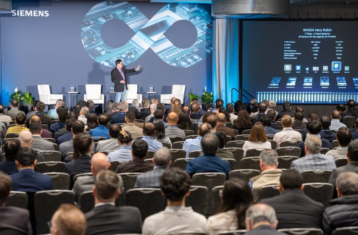
The semiconductor sector is moving beyond traditional electronic design automation toward a holistic, system‑level approach. AI is no longer a peripheral aid; it now serves as an engineering platform that can reason, plan, and execute tasks across design, verification, and packaging. NVIDIA’s vision of "agentic AI" enables autonomous optimization of SPICE simulations, optical proximity correction, and parasitic extraction, while Siemens leverages its industrial software suite to embed digital twins and thermal modeling directly into the chip‑design flow. This convergence blurs the line between hardware and software, demanding engineers who understand physics, AI, and cloud orchestration.
Cloud computing, championed by AWS, addresses the most acute bottleneck: time‑to‑market. A single‑quarter delay in launching a new AI‑optimized processor can translate into billions of dollars of lost revenue and excess energy consumption for hyperscale data‑center operators. By offering on‑demand, thousands‑of‑core GPU clusters, the cloud eliminates queuing delays that plague on‑premise EDA farms, enabling what AWS calls "speed‑of‑light" chip development. The elasticity of cloud resources also reduces capital outlay, as compute costs become a modest fraction of total design spend while delivering dramatically more iteration cycles per day.
The strategic implication is clear: semiconductor firms must embed AI, cloud, and digital‑twin capabilities into their core development processes or risk falling behind. Partnerships such as the NVIDIA‑Siemens integration illustrate a future where design, simulation, and manufacturing are tightly coupled in a single intelligent workflow. Companies that invest in these platforms can accelerate innovation, lower risk, and capture market share in the rapidly expanding AI hardware ecosystem. Executives should prioritize building cross‑functional teams that blend hardware expertise with AI and cloud engineering to stay competitive in this new era of semiconductor innovation.
Engineering the Next Era of Semiconductor Innovation
Comments
Want to join the conversation?