Google Launches TPU V8 Family: 8t Training Chip and 8i Inference Chip
Companies Mentioned
Why It Matters
The TPU v8 family redefines how cloud providers deliver AI acceleration. By separating training and inference into dedicated silicon, Google can optimize each workload for performance, power, and cost, potentially lowering the total cost of ownership for enterprises that rely on large‑scale models. The move also intensifies the hardware arms race with Nvidia and AMD, pushing the industry toward more specialized accelerators and tighter hardware‑software co‑design. For enterprises, the availability of a cloud‑native, end‑to‑end AI stack that includes custom CPUs, high‑bandwidth memory, and a proprietary interconnect could accelerate adoption of advanced AI agents, generative models, and real‑time analytics. At the same time, the strategic partnership with MediaTek and the shift to TSMC’s N3 node signal a broader diversification of the AI silicon supply chain, which may improve resilience and drive down costs over the next few years.
Key Takeaways
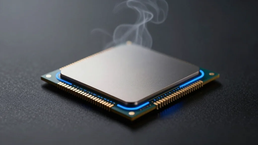
- •Google announced two new chips—TPU 8t (training) and TPU 8i (inference)—at Cloud Next 2026.
- •TPU 8t superpods scale to 9,600 chips and 2 PB of shared memory, delivering 12.6 FP4 PFLOPs per chip.
- •TPU 8i offers 10.1 FP4 PFLOPs, 288 GB HBM3E, and 384 MB on‑chip SRAM for ultra‑low‑latency inference.
- •Both chips are fabricated on TSMC’s N3 process; MediaTek joins Broadcom as a silicon design partner.
- •Google’s network can scale to 1 million TPUs per cluster, positioning the company against Nvidia’s Vera Rubin and AMD’s MI455X.
Pulse Analysis
Google’s bifurcated TPU strategy reflects a broader industry trend toward workload‑specific accelerators. Historically, the TPU line has been a single‑purpose device that attempted to serve both training and inference, but the widening gap between model size, training cost, and inference latency has made that compromise less tenable. By delivering a training‑focused 8t and an inference‑focused 8i, Google can push each silicon design to its performance envelope while still leveraging a unified software stack (TensorFlow, JAX, and the TPU runtime). This approach mirrors Nvidia’s recent split between its H100/H200 data‑center GPUs and the more cost‑effective T4/Tesla line, suggesting that specialization is becoming a competitive necessity.
The hardware choices also reveal Google’s cost calculus. Opting for HBM3E instead of the newer HBM4 reduces wafer cost and improves yield, allowing Google to price the TPU pods more aggressively. Coupled with the Boardfly interconnect and integrated power management, the v8 family promises higher compute‑per‑watt ratios, a critical metric for hyperscale data centers where electricity bills dominate OPEX. Enterprises that are sensitive to energy consumption—such as financial services and large‑scale SaaS providers—may find the TPU v8’s efficiency compelling enough to shift workloads from on‑prem GPUs to Google Cloud.
Finally, the partnership with MediaTek signals a strategic diversification of Google’s silicon ecosystem. By bringing a second design house into the fold, Google reduces its reliance on Broadcom and gains access to MediaTek’s expertise in low‑power ARM cores, which could accelerate future generations of custom CPUs (the Axion line). This diversification may also foster more competitive pricing for the silicon itself, a benefit that could cascade down to cloud customers. In the next 12‑18 months, the real test will be whether the performance and cost claims hold up in production workloads, and whether enterprises are willing to commit to a fully integrated Google stack despite potential lock‑in concerns.
Google Launches TPU v8 Family: 8t Training Chip and 8i Inference Chip
Comments
Want to join the conversation?
Loading comments...