Harvard Team Achieves Milliwatt UV Light Generation On a Photonic Chip
Why It Matters
By achieving milliwatt‑level UV output on a photonic chip, the work clears a key hurdle for scaling trapped‑ion quantum processors and miniaturizing UV‑based sensing and manufacturing tools, opening new commercial pathways for integrated photonics.
Key Takeaways
- •Harvard chip produces 4.2 mW UV at 390 nm
- •Sidewall poling achieves uniform domain inversion across waveguide
- •Output 120× previous thin‑film lithium niobate UV sources
- •Enables scalable trapped‑ion quantum computers and compact sensors
- •Shows lithium niobate can host integrated UV photonics
Pulse Analysis
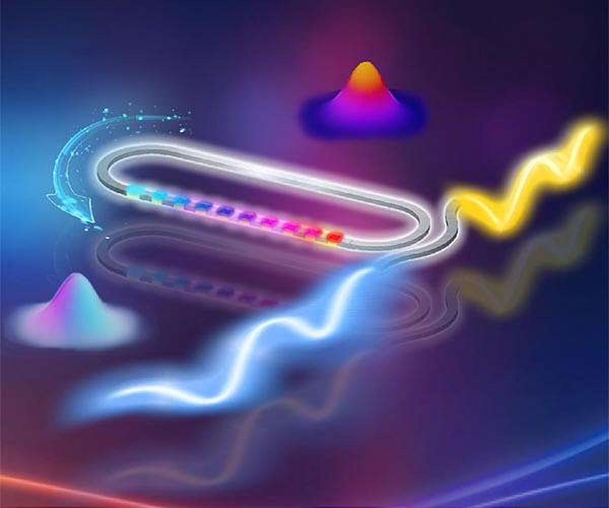
Integrated ultraviolet sources have long been a missing piece in the photonics toolbox, largely because UV photons are absorbed quickly in conventional waveguides. The Harvard team’s approach sidesteps this limitation by converting readily available red light into UV directly on the chip, leveraging the strong nonlinear properties of lithium niobate. This method not only simplifies the optical layout—eliminating bulky external UV lasers—but also aligns with the broader industry push toward monolithic photonic integration for faster, more reliable systems.
The core of the achievement lies in the newly introduced sidewall‑poling process. By placing metal electrodes directly against the etched waveguide walls, the researchers attained sub‑50 nm alignment accuracy, enabling full‑cross‑section domain inversion. This uniform poling maximizes the overlap between the optical mode and the nonlinear crystal regions, driving conversion efficiencies that push output power into the milliwatt regime. Compared with earlier thin‑film lithium niobate attempts that stalled at tens of microwatts, the 4.2 mW output represents a 120‑fold leap, effectively bridging the gap between laboratory proof‑of‑concepts and deployable technology.
The implications extend beyond academic interest. Scalable trapped‑ion quantum computers require compact, stable UV light at specific wavelengths, and chip‑scale sources could dramatically shrink system footprints and reduce costs. Likewise, portable environmental sensors and next‑generation photolithography tools stand to benefit from on‑chip UV generation, enabling faster deployment and lower power consumption. Backed by funding from the Air Force, Navy, NASA, and NSF, this advancement positions lithium niobate as a versatile platform for future UV‑centric applications, signaling a new era for integrated photonic devices.
Harvard Team Achieves Milliwatt UV Light Generation On a Photonic Chip
Comments
Want to join the conversation?
Loading comments...