Hiring for Precision: Why Thermal Stability Expertise Is the New Must-Have in Semiconductor Talent
Why It Matters
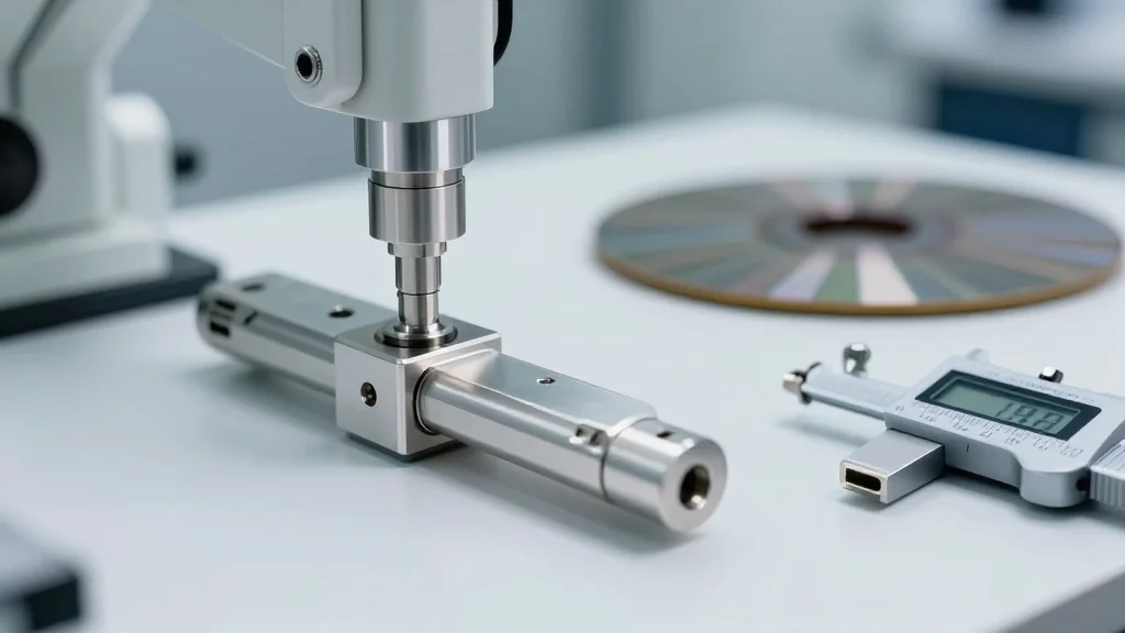
Thermal distortion directly threatens wafer alignment tolerances, driving costly scrap and downtime; mastering material and machining expertise is a competitive differentiator for fabs seeking higher yields and lower operating costs.
Key Takeaways
- •Aluminum 6061 warps 42 μm, causing $2.3 M yield loss.
- •PEEK reduces thermal distortion 73% with lower modulus despite higher CTE.
- •Low‑stress CNC parameters cut residual stress up to 55%.
- •Invar, ceramics, carbon composites offer sub‑5 μm expansion for critical features.
Pulse Analysis
Thermal stability has moved from a niche engineering concern to a strategic priority in semiconductor manufacturing. As wafer sizes expand and alignment tolerances tighten to sub‑10 μm, even modest thermal expansion can trigger misregistration, contamination, and costly yield penalties. The Arizona fab incident illustrates how a seemingly routine material choice—aluminum 6061—can become a liability when its 23.6 ppm/°C CTE interacts with residual stresses from aggressive CNC machining, leading to dimensional drift that exceeds the ±15 μm tolerance of wafer handling arms.
To mitigate these risks, fabs are increasingly turning to high‑performance engineering plastics such as PEEK and PPS, which, despite higher nominal CTEs, exhibit lower elastic modulus and superior stress‑relaxation characteristics. This combination yields a net reduction in effective distortion, as demonstrated by a 73 % improvement in dimensional stability and an eight‑month ROI after replacing aluminum components. Low‑CTE metals like Invar, advanced ceramics, and carbon‑fiber composites are reserved for the most critical alignment features, balancing cost against performance. The material shift also brings ancillary benefits: improved chemical resistance, outgassing performance below 10⁻⁸ torr·L/s, and inherent electrical insulation, all of which align with cleanroom and vacuum requirements.
Equally vital is the adoption of stress‑minimized machining protocols. Reducing cutting speeds, employing shallow passes, using sharp tooling, and integrating cryogenic or mist cooling can slash residual stresses by over 50 %. Post‑machining heat treatments further relax internal stresses before final inspection. Coupled with rigorous thermal cycling validation—500 to 5,000 cycles spanning -40 °C to +150 °C—these practices ensure components remain within ±10 μm dimensional change limits. Companies that embed this expertise into their talent pool gain a decisive edge, delivering higher yields, lower scrap rates, and faster time‑to‑market for next‑generation semiconductor devices.
Hiring for Precision: Why Thermal Stability Expertise Is the New Must-Have in Semiconductor Talent
Comments
Want to join the conversation?
Loading comments...