HRL’s T3L 40nm GaN-on-SiC Technology Achieves Manufacturing Readiness Level 6
Companies Mentioned
Why It Matters
Reaching MRL‑6 validates a domestic, high‑performance RF GaN supply chain, reducing reliance on foreign fabs and accelerating advanced defense and commercial applications.
Key Takeaways
- •HRL reaches MRL‑6 for 40 nm GaN‑on‑SiC process.
- •Production shift to MACOM enables high‑volume US domestic supply.
- •Open MPW access supports rapid prototyping for defense and commercial users.
- •Process compatible with 3D heterogeneous integration for smaller, lighter radar.
- •HRL offers low‑volume engineering foundry for qualified customers.
Pulse Analysis
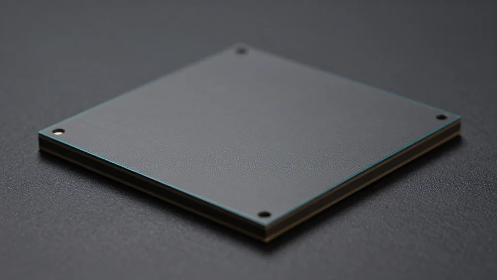
The 40 nm T3L gallium‑nitride on silicon‑carbide (GaN‑on‑SiC) platform announced by HRL Laboratories marks a pivotal step in U.S. semiconductor maturity. Achieving Manufacturing Readiness Level 6 under the Department of War’s validation program demonstrates that the process can be run on production‑relevant fab lines with repeatable control and a stable supply chain. For defense applications, this translates into a reliable source of high‑power, high‑frequency RF components that meet stringent performance and security standards, while commercial users gain access to a technology capable of delivering superior efficiency at millimeter‑wave frequencies.
HRL’s decision to hand high‑volume manufacturing to MACOM Technology Solutions creates a domestic production pipeline that reduces reliance on overseas foundries. The arrangement preserves HRL’s low‑volume engineering services and multi‑project wafer (MPW) access, allowing startups and defense contractors to prototype new designs without large upfront commitments. By coupling an open‑access MPW model with a scalable foundry partner, the ecosystem lowers entry barriers and accelerates time‑to‑market for next‑generation radar, satellite communications, and 5G/6G front‑end modules. This alignment with U.S. strategic supply‑chain goals is likely to attract additional government funding.
The T3L process is also engineered for advanced heterogeneous integration, including three‑dimensional (3DHI) architectures that stack digital control electronics directly onto the GaN power stage. This capability shrinks system size, weight and power (SWaP), a critical metric for airborne and space‑borne platforms. As antenna arrays and beam‑forming networks demand ever‑higher channel counts, the ability to embed GaN devices within compact modules gives designers a path to higher output power without proportional growth in thermal load. Industry analysts expect the technology to spur a new class of compact, energy‑efficient RF systems across both defense and high‑performance commercial markets.
HRL’s T3L 40nm GaN-on-SiC technology achieves Manufacturing Readiness Level 6
Comments
Want to join the conversation?
Loading comments...