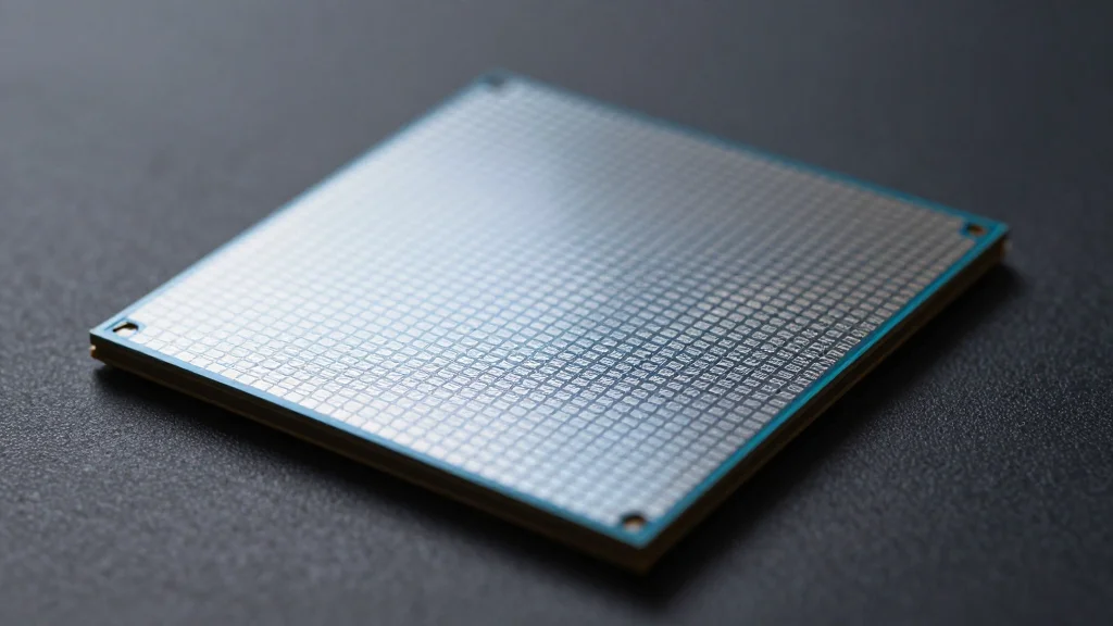
Huawei Claims 1.4nm-equivalent Chips by 2031, Narrowing Gap with TSMC

Companies Mentioned
Taiwan Semiconductor Manufacturing Company
TSM

Semiconductor Manufacturing International Corp.
Why It Matters
Huawei’s claim signals a potential shift in how advanced chips can be built without relying on EUV lithography, a technology tightly controlled by the United States and its allies. By focusing on signal‑time reduction rather than pure transistor scaling, the company may open a new design frontier that other constrained players could emulate, reshaping the competitive balance in AI hardware. If Huawei delivers on its 1.4‑nm‑equivalent promise, Chinese AI firms could source domestically‑designed processors that rival those from Nvidia, AMD and TSMC, reducing the strategic leverage the U.S. holds over China’s AI ambitions. The move also pressures the global foundry ecosystem, forcing leaders like TSMC and Samsung to accelerate architecture‑level innovations to stay ahead of a potentially self‑sufficient Chinese challenger. The breakthrough could also influence policy debates in Washington, where lawmakers weigh the merits of further tightening export controls against the risk of accelerating a parallel semiconductor ecosystem in China.
Key Takeaways
- •Huawei targets 1.4nm-equivalent transistor density by 2031 using the Tau Scaling Law.
- •LogicFolding architecture will debut in Kirin smartphones later in 2026 and in Ascend AI chips by 2030.
- •Company has designed and mass‑produced 381 chips over the past six years under the new principle.
- •TSMC plans 1.4nm mass production in 2028, giving Huawei a three‑year lead‑gap to close.
- •U.S. sanctions block Huawei from EUV lithography, prompting the architecture‑centric workaround.
Pulse Analysis
Huawei’s announcement reflects a strategic pivot from the traditional node‑centric race that has defined the semiconductor industry for decades. By betting on time‑based scaling, the firm is essentially acknowledging the physical limits of Moore’s Law and the geopolitical choke points around EUV equipment. This mirrors a broader industry trend where players such as Intel, AMD and Nvidia are investing heavily in chiplet integration, advanced packaging and heterogeneous architectures to sustain performance gains.
Historically, China’s semiconductor ambitions have been hampered by a lack of access to cutting‑edge lithography, forcing it to rely on older nodes and domestic foundries like SMIC. Huawei’s claim, if substantiated, could validate a new design‑first approach that sidesteps the need for the most advanced fabs. That would not only accelerate China’s AI hardware independence but also create a template for other sanctioned entities to follow, potentially fracturing the global supply chain into parallel ecosystems.
From a market perspective, the timing is critical. Nvidia and AMD are racing to capture the emerging “agentic AI” CPU market, while TSMC is expanding capacity to meet surging demand for 3‑nm and 2‑nm wafers. Huawei’s push could force foundries to offer more flexible design services and co‑development models, blurring the line between fab‑only and integrated device manufacturers. In the short term, investors will watch SMIC’s stock, the rollout of the LogicFolding‑based Kirin chip, and any U.S. policy responses. In the longer run, the success or failure of the Tau Scaling Law will shape whether architecture‑centric innovation can truly compensate for the loss of the most advanced manufacturing tools.
Huawei claims 1.4nm-equivalent chips by 2031, narrowing gap with TSMC
Comments
Want to join the conversation?
Loading comments...