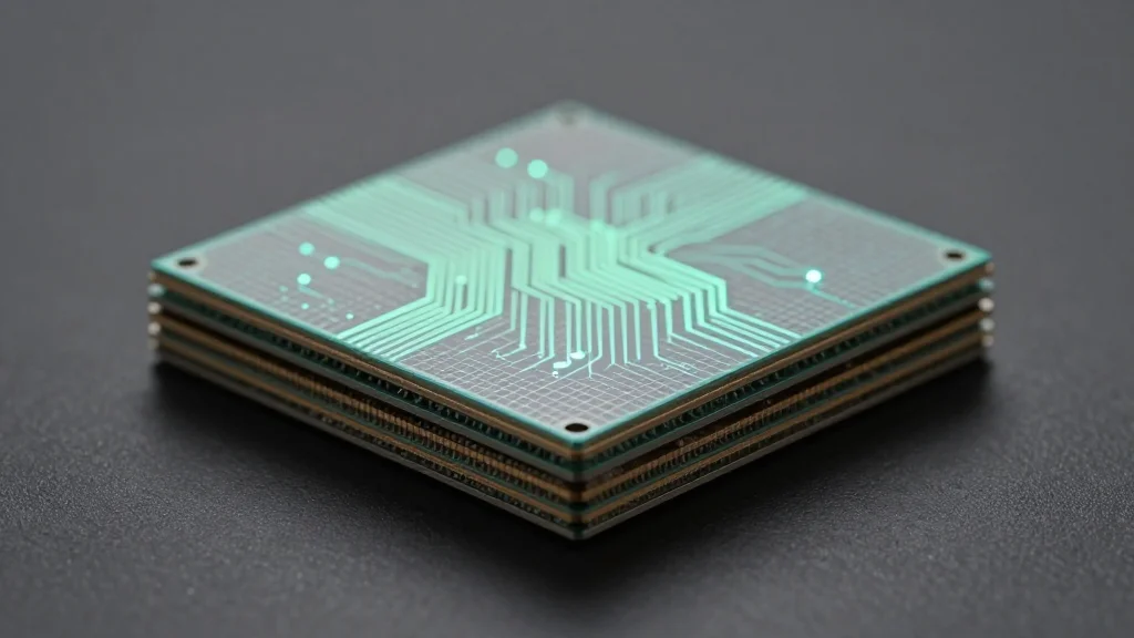
Huawei Unveils 'LogicFolding' Chip Design to Target 1.4nm Performance by 2031

Companies Mentioned

Why It Matters
Huawei's LogicFolding strategy could alter the balance of power in the global semiconductor ecosystem. By pursuing a performance path that sidesteps EUV lithography, the company aims to reduce China's dependence on foreign equipment and narrow the gap with industry leaders like TSMC and Samsung. If the architecture proves viable at scale, it may enable Chinese firms to field AI accelerators and high‑performance processors that rival those built on the most advanced nodes, reshaping supply‑chain geopolitics and influencing future export‑control policies. Beyond the immediate competitive implications, the move signals a broader shift toward architectural innovation as a lever for performance gains. As Moore's Law slows, other players—Intel, AMD, and emerging Chinese startups—are exploring 3‑D stacking, chiplet integration, and new interconnect standards. Huawei's public commitment adds momentum to this trend and could accelerate industry investment in design‑centric solutions that are less vulnerable to equipment bans.
Key Takeaways
- •Huawei announced the LogicFolding stacked‑architecture approach at a Shanghai conference on May 24, 2026
- •The roadmap targets 1.4‑nanometer‑class transistor density by 2031, five years after the announcement
- •Current Chinese fabs are estimated at ~7nm, while TSMC plans 1.4nm production in the next few years
- •LogicFolding aims to bypass EUV lithography, which is restricted under U.S. sanctions since 2019
- •Analysts warn that manufacturing challenges—thermal, yield, and integration—remain critical to realizing the claimed performance
Pulse Analysis
Huawei’s LogicFolding announcement reflects a strategic pivot from pure process scaling to architectural ingenuity, a trend that has been gathering steam as Moore's Law reaches its physical limits. By stacking functional layers and redefining data pathways, Huawei is betting that efficiency gains can offset the raw transistor count advantage held by TSMC and Samsung. Historically, similar 3‑D approaches—such as Intel’s Foveros and TSMC’s CoWoS—have delivered modest performance lifts but required mature manufacturing ecosystems to be cost‑effective. Huawei’s challenge is twofold: first, to prove that its stacked design can be fabricated on a 7nm‑class process without prohibitive thermal penalties; second, to secure a supply chain that can produce the necessary high‑precision interconnects under U.S. export controls.
If Huawei can deliver a working prototype by 2027, the ripple effects could be profound. Chinese AI startups would gain access to home‑grown high‑performance chips, reducing reliance on imported GPUs and potentially lowering the cost of training large models. Moreover, the success of a design‑centric roadmap could inspire other sanctioned entities to double‑down on architecture, prompting a wave of patents and standards that sidestep traditional lithography bottlenecks. Conversely, failure to translate the concept into silicon would reinforce the prevailing view that without cutting‑edge fabs, architectural tricks alone cannot close the performance gap.
From a policy perspective, the LogicFolding narrative challenges the efficacy of export controls that focus on equipment rather than design. Washington may need to broaden its toolkit to include design‑software licensing and intellectual‑property enforcement if architectural workarounds become a mainstream path for sanctioned firms. The coming months—particularly the IEEE symposium paper and early‑2027 prototype runs—will be the litmus test for whether Huawei’s vision is a genuine breakthrough or a high‑profile PR maneuver.
Huawei Unveils 'LogicFolding' Chip Design to Target 1.4nm Performance by 2031
Comments
Want to join the conversation?
Loading comments...