Huawei Unveils Tau Scaling Law, Targets 1.4nm‑Equivalent Chips by 2031
Companies Mentioned
Why It Matters
The Tau Scaling Law represents a strategic pivot for China’s semiconductor sector, offering a path to high‑density, high‑efficiency chips without the costly EUV equipment that has been blocked by U.S. export controls. By focusing on system‑level latency rather than geometric scaling, Huawei aims to keep Chinese devices competitive in smartphones, AI inference, and telecom infrastructure, sectors that together account for a large share of global chip demand. If successful, the approach could erode the technological advantage held by TSMC and Nvidia, reshaping the competitive dynamics of the global chip market. It also signals to other nations, especially in the Global South, that a viable alternative to the traditional Moore’s Law trajectory exists, potentially accelerating the diffusion of advanced semiconductor capabilities beyond the traditional hubs of the United States, Taiwan, and South Korea.
Key Takeaways
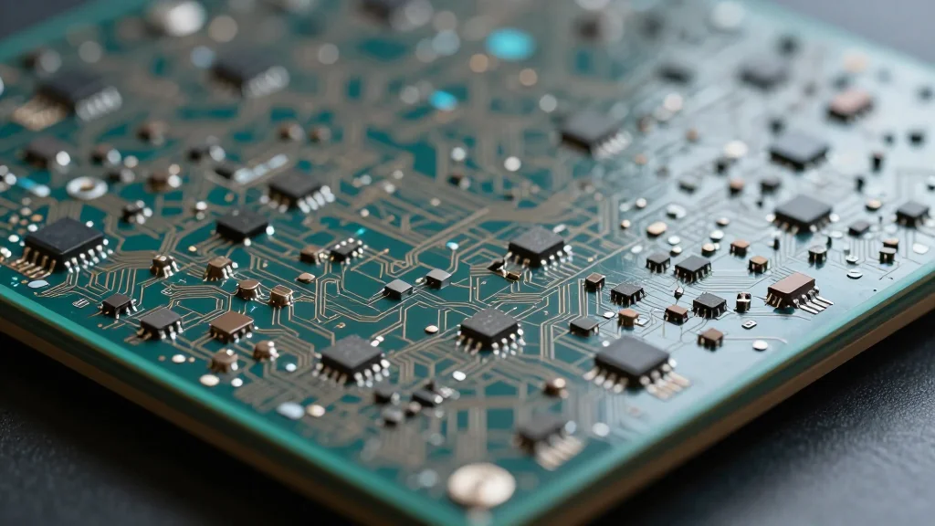
- •Huawei announced the Tau (τ) Scaling Law, targeting 1.4nm‑equivalent transistor density by 2031.
- •Over 380 chip products have already entered mass production using the new architecture.
- •LogicFolding, the core technique, claims >50% density boost and 41% energy‑efficiency gain at the same node.
- •Nvidia CEO Jensen Huang said the breakthrough is not a threat to TSMC’s 3D packaging expertise.
- •Analysts predict the move could reduce U.S. export‑control leverage and spur domestic chip investment in China.
Pulse Analysis
Huawei’s Tau Scaling Law is less a technological miracle than a pragmatic response to a constrained ecosystem. By re‑orienting design priorities toward latency and system‑level integration, the company sidesteps the exponential cost curve of sub‑3nm EUV lithography, which has become a geopolitical choke point. This mirrors historical shifts where industry bottlenecks forced new architectures—think of the rise of multi‑core CPUs when clock speeds plateaued. The real test will be whether the promised density gains translate into real‑world yields and power budgets that meet the expectations of AI and telecom customers.
From a market perspective, the announcement could catalyze a bifurcation of the semiconductor landscape. The high‑performance track, led by TSMC and Nvidia, will likely continue to chase absolute performance at premium prices, while the “inclusive” track championed by Huawei, SMIC, and their partners may capture price‑sensitive segments in emerging markets. If Huawei can deliver on its timeline, it may force Western foundries to reconsider the economics of offering lower‑cost, mature‑node services to Chinese customers, potentially opening a new revenue stream that balances the current high‑margin, high‑risk advanced‑node business.
Strategically, the Tau law also serves as a narrative device for Beijing, showcasing domestic ingenuity in the face of sanctions. The symbolism—drawing parallels to ancient engineering feats and framing the effort as a “Long March” of science—reinforces political messaging that technology independence is achievable. However, the path ahead is fraught with technical hurdles: thermal management of densely stacked layers, the need for new EDA toolchains, and the risk that yields may lag behind expectations. Investors and policymakers will be watching the first Kirin rollout closely; its performance and reliability will likely set the tone for whether the Tau Scaling Law becomes a cornerstone of China’s semiconductor future or a well‑publicized experiment that falls short of its lofty claims.
Huawei Unveils Tau Scaling Law, Targets 1.4nm‑Equivalent Chips by 2031
Comments
Want to join the conversation?
Loading comments...