KnowMade Details a Rapidly Evolving Role for GaN
Why It Matters
The accelerating GaN innovation pipeline signals imminent shifts in AI datacenter power, high‑voltage conversion, and advanced photonics, while emerging IP and trade conflicts could reshape global supply chains and market leadership.
Key Takeaways
- •327 papers and 362 patents on GaN published this month
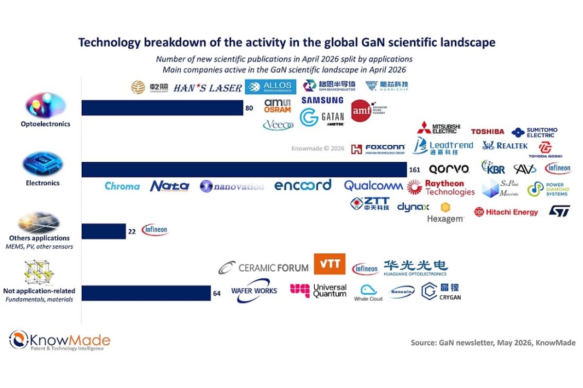
- •Electronics dominate GaN activity: 162 papers, 238 patents; optoelectronics also strong
- •MicroLEDs move from displays to AI optical interconnects and biomedical uses
- •Vertical GaN devices surpass 10 kV breakdown, enabling high‑voltage conversion
- •Infineon vs Innoscience patent fight highlights GaN’s geopolitical supply‑chain risk
Pulse Analysis
The GaN sector is entering a phase of rapid expansion, driven by a record influx of academic papers and patent filings. Over 300 new scientific studies and more than 350 patents appeared in a single month, reflecting heightened competition among semiconductor firms and research institutions. This momentum is fueled by the material’s ability to operate at higher voltages and frequencies than silicon, making it a prime candidate for AI‑intensive datacenters, electric‑vehicle powertrains, and next‑generation telecom infrastructure. As manufacturers push GaN from niche RF amplifiers into broader power‑electronics platforms, the technology is poised to become a cornerstone of high‑density, energy‑efficient computing.
In the optoelectronics arena, micro‑LEDs are shedding their traditional display‑only image and emerging as versatile photonic building blocks. Recent collaborations have demonstrated flexible InGaN micro‑LED arrays for neural stimulation, hybrid laser‑diode integration on silicon photonics, and high‑efficiency red emitters for full‑color displays. These advances not only improve optical performance but also align with existing semiconductor manufacturing lines, accelerating the path toward commercial AR/VR headsets, biomedical sensors, and ultra‑low‑power optical interconnects inside AI servers. The convergence of micro‑LEDs with AI workloads underscores a broader trend: photonic communication is becoming a strategic solution to the thermal and bandwidth limits of copper interconnects.
Meanwhile, the electronics side of GaN is achieving milestones that were once speculative. Vertical GaN‑on‑GaN diodes now exceed 10 kV breakdown, unlocking new possibilities for medium‑ and high‑voltage converters in EV charging and grid‑scale storage. At the same time, patent battles such as the Infineon‑Innoscience dispute highlight how geopolitical considerations are inseparable from technical progress. Supply‑chain sovereignty, export controls, and IP enforcement are shaping where and how GaN fabs are built, influencing the competitive landscape for AI datacenter power modules and defense electronics. Companies that can secure both advanced device architectures and resilient supply chains will likely dictate the next wave of GaN‑driven innovation.
KnowMade details a rapidly evolving role for GaN
Comments
Want to join the conversation?
Loading comments...