LUBIS EDA: Addressing the Verification Bottleneck in Modern Chip Design
•February 19, 2026
0
Why It Matters
By turning verification from a risk‑laden bottleneck into an automated, measurable step, LUBIS EDA helps semiconductor firms cut development costs and meet aggressive product schedules, a critical advantage in the fast‑moving AI and autonomous systems markets.
Key Takeaways
- •Verification bottleneck slows chip design cycles.
- •Formal verification finds corner‑case bugs simulation misses.
- •LUBIS automates assertion generation, reducing manual effort.
- •Cloud‑based platform scales formal checks across designs.
- •Consulting services accelerate formal adoption in teams.
Pulse Analysis
The semiconductor industry faces an escalating verification challenge as chip architectures grow in complexity to support AI accelerators, autonomous vehicles, and edge computing. Traditional simulation‑based testbenches rely on constrained‑random stimuli, which often miss rare corner cases that can cause costly silicon failures. This verification gap not only inflates design cycles but also introduces significant financial risk, prompting designers to seek more exhaustive methods that can keep pace with aggressive time‑to‑market demands.
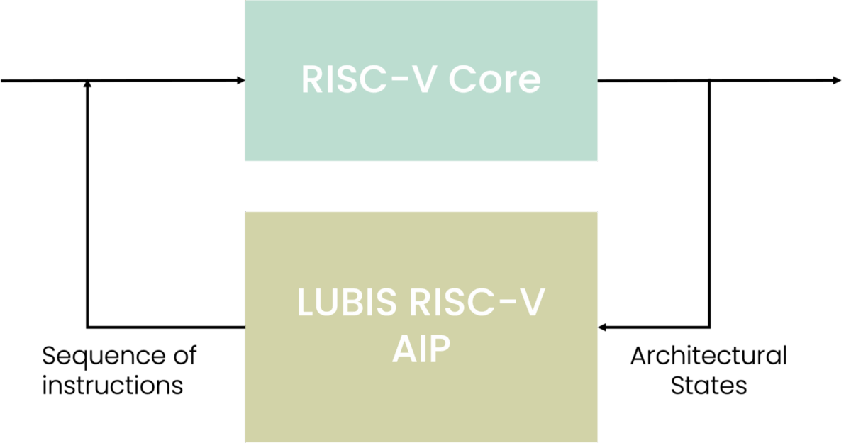
Formal verification provides mathematical proof that a design adheres to its specifications across all possible inputs and states, offering a level of confidence unattainable with simulation alone. LUBIS EDA’s platform streamlines this process by automatically generating assertions from reusable models, embedding formal‑ready environments into continuous‑integration pipelines, and delivering the tools via a cloud infrastructure that scales on demand. The combination of automation, cloud elasticity, and expert consulting reduces the expertise barrier, enabling design teams to integrate formal checks alongside traditional simulation without disrupting existing workflows.
The broader market implications are significant. As safety‑critical applications and high‑performance AI workloads dominate chip roadmaps, demand for scalable formal verification solutions is set to surge. Companies that adopt LUBIS’s automated, data‑driven verification ecosystem can expect faster design closure, fewer silicon respins, and stronger competitive positioning. Moreover, the shift toward service‑oriented EDA models—bundling software, cloud resources, and consultancy—signals a transformation in how verification tools are delivered, aligning with the industry’s move toward more agile, cost‑effective development practices.
LUBIS EDA: Addressing the Verification Bottleneck in Modern Chip Design
0
Comments
Want to join the conversation?
Loading comments...