Monash Researchers Unveil ‘Swiss‑Army‑Knife’ Optical Chip with 11 Functions
Why It Matters
The ability to embed multiple optical functions on a single chip addresses a critical bottleneck in photonic integration: the trade‑off between performance and footprint. Data‑center operators are under pressure to increase bandwidth while reducing power and cooling costs; a multifunctional metasurface directly tackles both challenges by eliminating redundant components. Moreover, the approach could accelerate the adoption of photonic technologies in sectors that have been limited by size and cost, such as point‑of‑care medical diagnostics and compact LIDAR systems for autonomous vehicles. Beyond immediate applications, the work signals a broader paradigm shift in nanophotonics. By proving that engineered disorder can outperform perfect order, the study invites researchers to revisit other optical architectures—filters, modulators, and sensors—with a fresh design lens. This could spur a wave of innovation that reshapes the hardware landscape of the entire optics industry.
Key Takeaways
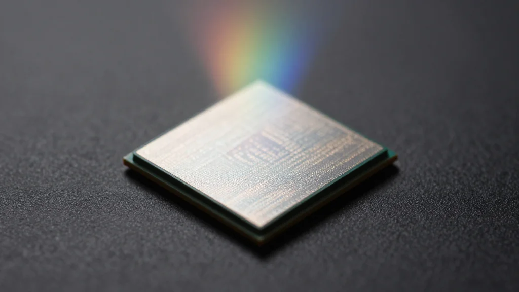
- •Monash University demonstrated a metasurface chip that integrates 11 broadband optical functions on a single surface.
- •The device operates across a 200 nm wavelength range (1200‑1400 nm) and includes focusing, dispersion control, and polarization analysis.
- •Researchers used a disordered mosaic pattern of meta‑pixels, challenging the conventional need for perfect periodicity.
- •Potential to replace multiple bulky components in telecom and data‑center transceivers, reducing size and power consumption.
- •Next steps include scaling to wafer‑level production and testing in real‑world wavelength‑division multiplexing links.
Pulse Analysis
The Monash metasurface represents more than a clever laboratory trick; it is a strategic lever for the photonics industry’s long‑standing scaling dilemma. Historically, adding new optical functions meant stacking additional elements, each with its own alignment tolerances and insertion loss. That incremental approach has hit diminishing returns as data‑center bandwidth demands outpace the physical limits of current modules. By collapsing eleven functions into a single planar device, the mosaic metasurface sidesteps the stacking penalty entirely, offering a path to denser, lower‑loss optical interconnects.
From a competitive standpoint, the technology could erode the market share of established component suppliers that specialize in discrete lenses, gratings, and polarizers. Companies that have invested heavily in precision assembly lines may need to pivot toward wafer‑scale metasurface fabrication or risk obsolescence. Conversely, firms with strong lithography capabilities—particularly those already producing silicon photonics—are well positioned to adopt the new design philosophy. The collaboration with the University of Exeter and the University of the Witwatersrand hints at a growing international ecosystem that could accelerate standard‑setting and supply‑chain development.
Looking ahead, the key risk lies in manufacturability. Translating a lab‑scale mosaic pattern into a high‑yield, cost‑effective process will require advances in nano‑imprint or extreme‑ultraviolet lithography. If those hurdles are cleared, the ripple effects could be profound: faster rollout of 400 G and beyond Ethernet, lighter payloads for satellite communications, and more compact optical sensors for medical and environmental monitoring. The chip’s versatility also opens cross‑industry licensing opportunities, turning a single breakthrough into a multi‑sector catalyst for hardware innovation.
Monash Researchers Unveil ‘Swiss‑Army‑Knife’ Optical Chip with 11 Functions
Comments
Want to join the conversation?
Loading comments...