NDS Taiwan to Showcase Integrated Warpage Control Solution for PLP at SEMICON SEA 2026
Why It Matters
Warpage is a primary yield limiter in panel‑level packaging; controlling it end‑to‑end unlocks higher throughput and cost efficiency for semiconductor manufacturers. NDS Taiwan's holistic method positions it as a key enabler of the industry’s shift from wafer‑ to panel‑based processes.
Key Takeaways
- •Integrated warpage control spans front‑end to debonding stages
- •Balance Film provides stress compensation during thermal cycles
- •Glass carrier temporary bonding stabilizes panels during thinning
- •Precision grinding reduces TTV and subsurface damage
- •Clean debonding preserves surface integrity for downstream RDL
Pulse Analysis
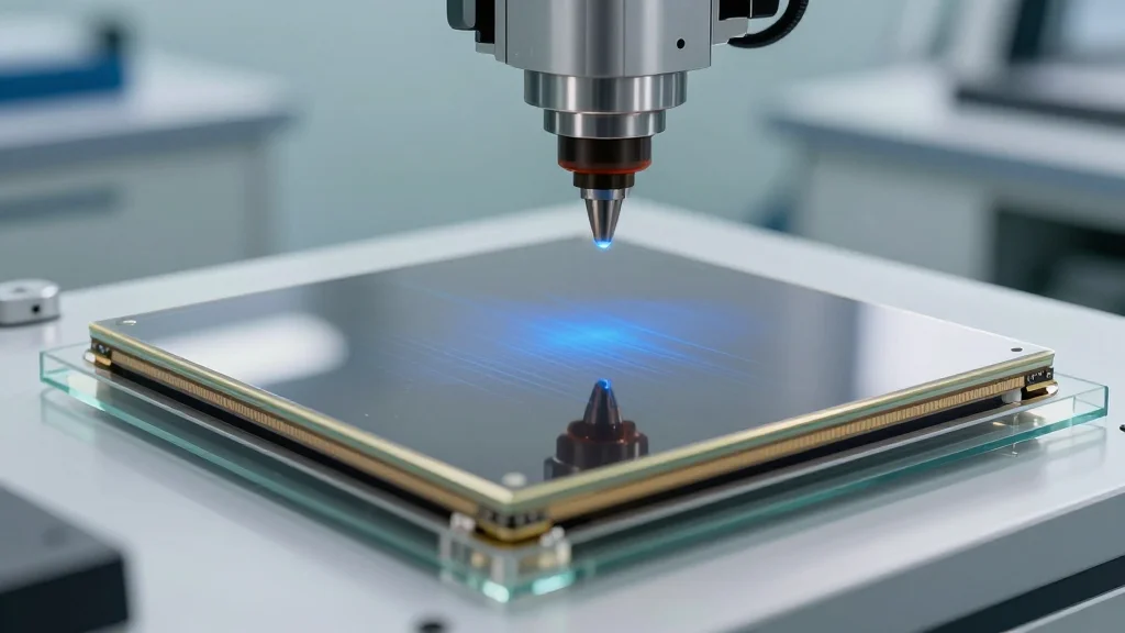
Panel‑level packaging (PLP) is rapidly supplanting traditional wafer‑level approaches as chip manufacturers chase higher density and lower cost per die. The transition, however, introduces pronounced warpage issues because larger silicon panels experience greater thermal and mechanical gradients during bonding, thinning and redistribution‑layer (RDL) formation. Unchecked warpage can misalign interconnects, increase defectivity and erode overall yield, making stress management a top priority for fabs and OSATs alike.
NDS Taiwan’s integrated warpage‑control solution tackles the problem by synchronizing material choices and equipment across the full PLP flow. A proprietary Balance Film acts as a stress‑compensation layer, while a temporary glass carrier supplies mechanical rigidity during aggressive thinning steps. High‑precision grinding ensures uniform thickness with minimal total‑target‑variation, and the polishing stage leverages optimized pads and slurry additives to achieve flatness required for fine‑pitch RDLs. The final clean debonding step removes the carrier without residue, preserving the panel surface for subsequent processes. This end‑to‑end methodology transforms warpage from a reactive fix into a predictable, controllable parameter.
The strategic timing of the showcase at SEMICON SEA 2026 underscores the market’s appetite for scalable PLP solutions. As Asian fabs expand capacity for 5G, AI and automotive chips, manufacturers that can guarantee stable yields will command premium positioning. NDS Taiwan’s presence at Booth 1640 signals its intent to partner with leading semiconductor players, offering a turnkey warpage‑control suite that can accelerate PLP adoption and drive down total cost of ownership. Industry observers will watch closely to see how quickly the solution translates into measurable yield improvements across high‑volume production lines.
NDS Taiwan to Showcase Integrated Warpage Control Solution for PLP at SEMICON SEA 2026
Comments
Want to join the conversation?
Loading comments...