NEO Semiconductor's Revolutionary 3D X-DRAM for AI Processors Has Passed Proof-of-Concept Validation — Company Secures Funding to Develop Next-Gen Memory HBM Alternative
Companies Mentioned
Why It Matters
The breakthrough could ease AI memory bottlenecks while reducing costs, challenging HBM's dominance in high‑performance computing.
Key Takeaways
- •3D X‑DRAM achieved sub‑10 ns read/write latency.
- •Retention exceeds 1 s at 85 °C, 15× JEDEC standard.
- •Endurance surpasses 10¹⁴ cycles, suitable for AI workloads.
- •Uses existing 3D NAND fab lines, reducing production cost.
- •Strategic funding led by Acer founder Stan Shih accelerates development.
Pulse Analysis
The surge in generative‑AI models has exposed a chronic memory bandwidth gap. While GPUs now deliver teraflops of compute, the DRAM stacks that feed them have struggled to keep pace, prompting designers to adopt high‑bandwidth memory (HBM). HBM’s performance is undeniable, but its 3‑D stacking, through‑silicon‑via interconnects and specialized packaging drive unit costs above $200 per gigabyte, limiting adoption in cost‑sensitive data‑center servers. Industry analysts therefore view a lower‑cost, high‑density DRAM alternative as a strategic priority.
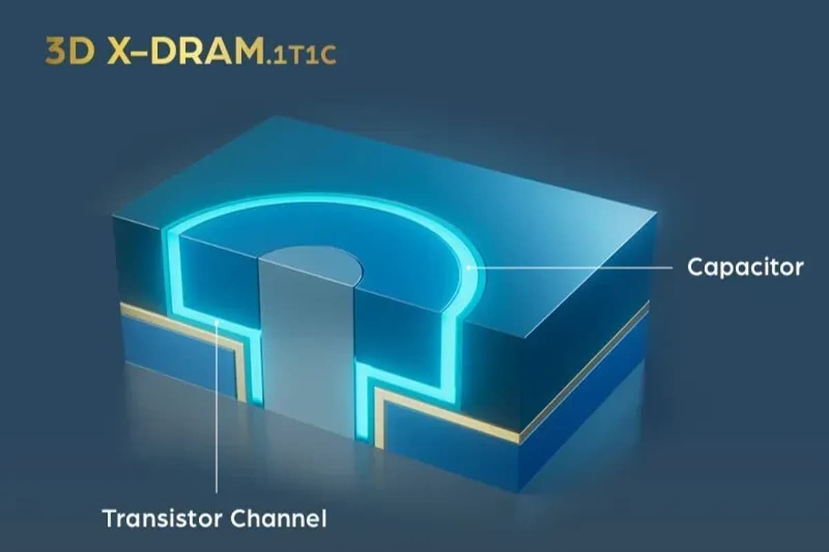
NEO Semiconductor’s 3D X‑DRAM attempts to meet that priority by repurposing mature 3D NAND fabrication lines. In a proof‑of‑concept run at Taiwan’s NIAR‑TSRI, the chips demonstrated read/write latency under 10 nanoseconds, data retention longer than one second at 85 °C—a fifteen‑fold improvement over JEDEC standards—and endurance exceeding 10¹⁴ cycles. Because the architecture builds memory cells directly into a monolithic vertical stack rather than bonding separate dies, it sidesteps the costly TSV and interposer steps that define HBM, potentially slashing production expenses.
The technology’s validation arrived alongside a strategic investment led by Stan Shih, the former Acer CEO and longtime TSMC board director, signaling confidence in a market that could soon demand a cheaper AI‑grade memory. NEO plans to license the process to established memory makers, positioning itself as a catalyst for a new ecosystem of 3‑D DRAM suppliers. If the company can translate POC performance into volume production, it could compress AI system costs, broaden access to large‑scale training, and reshape the competitive dynamics between DRAM, HBM, and emerging memory startups.
NEO Semiconductor's revolutionary 3D X-DRAM for AI processors has passed proof-of-concept validation — company secures funding to develop next-gen memory HBM alternative
Comments
Want to join the conversation?
Loading comments...