New Photonic Device Efficiently Beams Light Into Free Space
•March 11, 2026
0
Why It Matters
The technology provides a practical, scalable interface between integrated photonics and free‑space light, unlocking higher bandwidth interconnects for quantum processors and ultra‑compact optical systems. It also paves the way for next‑generation high‑resolution displays and miniature sensing devices.
Key Takeaways
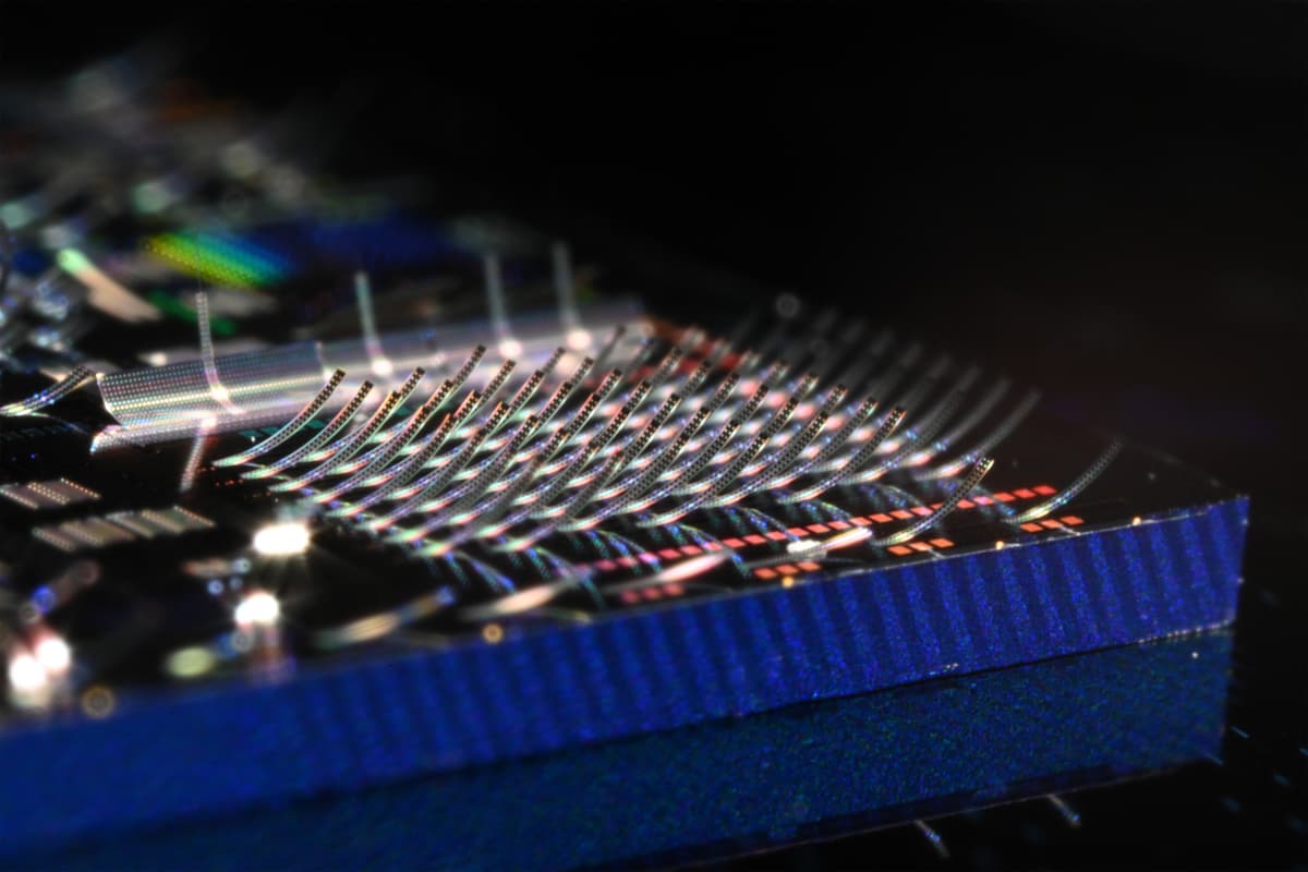
- •Upward‑curving “ski‑jump” emitters launch thousands of laser beams
- •Bimaterial strain creates scalable, self‑aligned photonic structures
- •Enables sub‑micron pixel density, surpassing smartphone displays
- •Allows simultaneous control of millions of diamond qubits
- •Potential for compact AR, Lidar, and high‑speed 3D printing
Pulse Analysis
Photonic integration has long promised faster data transport and lower power consumption, yet the bottleneck has been coupling light off the chip. Conventional grating couplers or edge emitters can only handle a handful of beams, limiting their usefulness for applications that require dense, free‑space illumination such as quantum control or high‑resolution projection. The new MIT‑led platform sidesteps these constraints by converting waveguide‑confined light into a dense array of free‑space beams, effectively turning a silicon wafer into a programmable light‑shooter. This breakthrough reshapes the design space for photonic systems that must interact with the external environment without sacrificing the compactness of on‑chip optics.
The core of the invention lies in a two‑layer, bimaterial structure that curls upward as it cools, forming microscopic “ski jumps.” By patterning silicon nitride and aluminum nitride with differing thermal expansion coefficients, the researchers induce a predictable strain that lifts each emitter into the third dimension. Integrated modulators then toggle each jump on or off, allowing precise color and intensity control across thousands of points. The result is a stable, error‑free projection capable of rendering images at a pixel density that dwarfs current smartphone screens—30,000 pixels in an area that would normally host just two. This level of control, achieved without active feedback, demonstrates that large‑scale, high‑resolution free‑space light sources can be fabricated using standard semiconductor processes.
Beyond the laboratory, the implications are far‑reaching. Quantum computers based on diamond nitrogen‑vacancy centers require individual laser addressing for millions of qubits; the ski‑jump array offers a path to that massive parallelism. In consumer tech, the same principle could drive ultra‑compact augmented‑reality glasses, miniature Lidar modules for autonomous drones, and faster, finer‑resolution 3D printers that cure resin with pinpoint laser spots. As the platform scales and yields improve, it may become the optical engine that unifies on‑chip photonics with the free‑space world, catalyzing new product categories and accelerating the adoption of photonic technologies across multiple industries.
New photonic device efficiently beams light into free space
0
Comments
Want to join the conversation?
Loading comments...