Purdue and Taiwan’s GCCS Partner to Scale Silicon Carbide Substrates to 8- and 12-Inches
Why It Matters
Scaling SiC wafers to larger diameters will lower costs and boost performance for AI data centers, power grids, and future 6G networks, strengthening U.S. tech security.
Key Takeaways
- •Purdue and GCCS aim for 8‑inch SiC wafers
- •12‑inch SiC scaling targets high‑power AI workloads
- •Collaboration includes workforce development for domestic SiC supply
- •Focus on defect reduction to boost manufacturing yields
- •SiC advances thermal management, power efficiency, 6G devices
Pulse Analysis
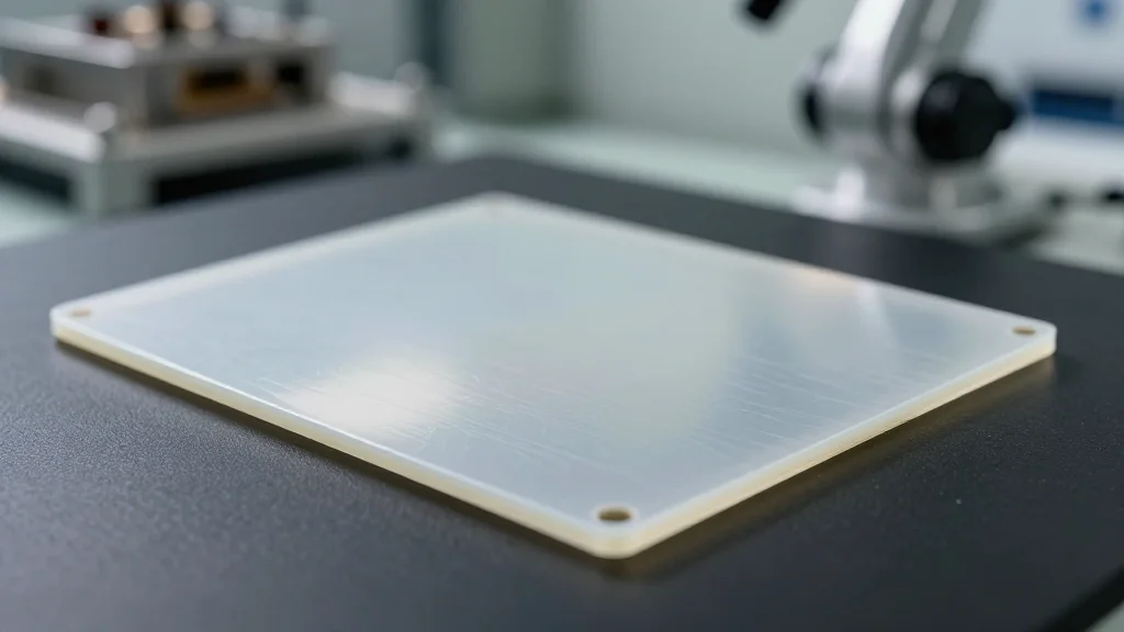
Silicon‑carbide is emerging as the material of choice for high‑power, high‑temperature electronics, offering superior thermal conductivity and breakdown voltage compared with traditional silicon. As AI models grow in size and data‑center power densities climb, manufacturers are hitting silicon’s physical limits, prompting a shift toward larger‑diameter SiC wafers that can host more devices per substrate and reduce per‑chip cost. The global SiC market, projected to exceed $10 billion by 2030, is being driven by demand from electric‑vehicle power modules, renewable‑energy converters, and next‑generation telecom equipment.
The Purdue‑GCCS alliance leverages Purdue’s Birck Nanotechnology Center—one of the nation’s most advanced academic cleanrooms—and GCCS’s expertise in crystal growth cultivated within Taiwan’s robust semiconductor ecosystem. Their five‑year MoU outlines joint R&D on defect isolation, crystal‑growth optimization, and scaling to 8‑inch and 12‑inch wafers, while also establishing a pipeline for training engineers skilled in SiC processing. By integrating academic research with industry‑scale manufacturing, the partnership aims to accelerate the transition from pilot‑line production to high‑volume commercial output.
Beyond technical gains, the collaboration addresses strategic concerns about supply‑chain resilience. Domestic SiC capacity reduces reliance on overseas sources, aligning with U.S. policy goals for semiconductor independence and national security. Successful scale‑up could lower the cost of high‑efficiency power converters for data‑center servers, improve thermal management in AI accelerators, and enable the power‑dense components required for 6G radio access networks. As the ecosystem matures, the Purdue‑GCCS model may become a template for other university‑industry partnerships seeking to fast‑track critical materials into the market.
Purdue and Taiwan’s GCCS partner to scale silicon carbide substrates to 8- and 12-inches
Comments
Want to join the conversation?
Loading comments...