Quantum‑dot Spin Qubits Move without Loss, Boosting Scalable Error‑corrected Designs
Why It Matters
The ability to move spin qubits across a semiconductor chip without decoherence addresses a core bottleneck in building large‑scale quantum computers. Error‑corrected logical qubits require thousands of physical qubits arranged in flexible topologies; until now, silicon‑based platforms struggled to provide the necessary connectivity without resorting to complex, non‑scalable hardware. By uniting mass‑manufacturable quantum dots with on‑chip transport, the discovery could compress the development timeline for fault‑tolerant quantum processors and lower the cost barrier for entry. Beyond the immediate technical impact, the result may shift investment patterns within the quantum hardware ecosystem. Venture capital and corporate R&D funds have been split between ion‑trap, photonic, and semiconductor approaches. Demonstrating that semiconductor qubits can achieve both scalability and connectivity could attract additional capital to chip‑focused startups and encourage established semiconductor firms to accelerate their quantum roadmaps.
Key Takeaways
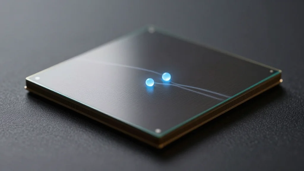
- •Researchers demonstrated lossless transport of spin qubits between quantum dots on a silicon chip.
- •Quantum‑dot architecture enables bulk manufacturing using existing semiconductor fabs.
- •On‑chip mobility offers any‑to‑any qubit connectivity traditionally limited to atom‑based systems.
- •The breakthrough supports surface‑code error‑correction schemes that need flexible entanglement.
- •Next milestones include scaling the shuttle operation to multi‑dot arrays and integrating high‑fidelity gates.
Pulse Analysis
The new quantum‑dot shuttle experiment arrives at a pivotal moment when the quantum hardware race is fragmenting into distinct technology camps. Silicon‑based approaches have long promised economies of scale, but their qubits have been hamstrung by limited interconnectivity, forcing designers to adopt rigid lattice structures. By proving that a spin qubit can be physically relocated without decoherence, the research collapses that divide, allowing silicon processors to emulate the flexible wiring of ion‑trap systems while retaining the cost advantages of CMOS fabrication.
Historically, error‑corrected quantum computing has been anchored to the surface code, which thrives on a two‑dimensional grid with nearest‑neighbor gates but also benefits from occasional long‑range links to reduce overhead. The shuttle capability effectively creates those long‑range links on a chip, potentially slashing the number of physical qubits required per logical qubit. If the error rates during transport remain below the fault‑tolerance threshold—currently estimated around 10⁻³ per operation—designers can dramatically simplify control electronics and reduce the cryogenic wiring burden that has plagued large ion‑trap arrays.
From a market perspective, the development could re‑balance funding flows. Investors have poured billions into ion‑trap firms like IonQ and photonic startups such as PsiQuantum, betting on their intrinsic connectivity. A proven semiconductor pathway that offers comparable flexibility may redirect capital toward companies like Intel, IBM, and a new wave of quantum‑dot specialists. Moreover, the compatibility with existing fabs could accelerate time‑to‑market, giving early adopters a competitive edge in the emerging quantum cloud services arena. The next year will likely see a surge in prototype chips that integrate shuttle mechanisms with high‑fidelity two‑qubit gates, setting the stage for the first error‑corrected logical qubits to be demonstrated on a silicon platform.
Quantum‑dot spin qubits move without loss, boosting scalable error‑corrected designs
Comments
Want to join the conversation?
Loading comments...