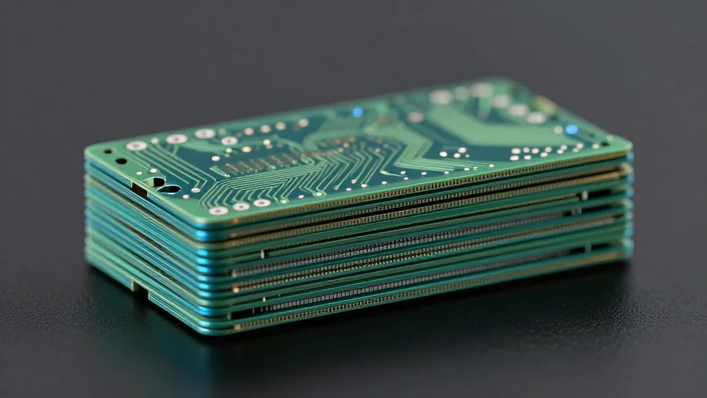
Samsung Ships First 12‑Layer HBM4E Samples, Boosting AI Memory Bandwidth

Companies Mentioned
Why It Matters
The HBM4E launch raises the performance ceiling for AI training and inference, enabling larger models to run faster and more efficiently. By delivering a 30% capacity boost and a 20% speed increase, Samsung directly addresses the memory bottleneck that has limited the scaling of large language models, potentially accelerating breakthroughs in natural language processing, scientific simulation, and real‑time analytics. In the broader hardware ecosystem, the move signals a tightening of the memory supply chain, where Samsung’s integrated approach—combining DRAM, logic, and advanced packaging—could set a new standard for end‑to‑end semiconductor solutions. Competitors will need to accelerate their own high‑bandwidth memory programs or risk losing design wins in next‑generation AI accelerators, influencing investment decisions across the AI hardware stack.
Key Takeaways
- •Samsung begins shipping 12‑layer HBM4E samples, the first of its generation.
- •HBM4E offers 48 GB capacity per stack, a 30% increase over HBM4.
- •Peak bandwidth reaches 3.6 TB/s per stack with 14 Gbps pin speed, scalable to 16 Gbps.
- •Power consumption cut by 16% and thermal resistance improved >14% versus prior models.
- •Samsung plans 32 GB (8‑layer) and 64 GB (16‑layer) variants to meet diverse AI workloads.
Pulse Analysis
Samsung’s early shipment of HBM4E samples is more than a product launch; it’s a strategic maneuver to lock in the memory architecture of the next wave of AI hardware. Historically, memory bandwidth has been a limiting factor for scaling large language models, forcing designers to trade off model size for speed or to over‑provision cooling. By delivering a 20% speed uplift and a 30% capacity jump while simultaneously improving energy efficiency, Samsung removes a key constraint, allowing AI chip designers to push performance envelopes without proportionally increasing power budgets.
The competitive landscape intensifies as Micron and SK Hynix scramble to catch up. Both firms have announced roadmaps for HBM5, but those timelines extend into 2027, giving Samsung a multi‑year head start. This advantage could translate into design wins for major GPU vendors like NVIDIA and AMD, as well as for custom AI accelerators from startups and hyperscalers. The ripple effect may also influence foundry demand; Samsung’s 4 nm logic base die integration showcases a vertically integrated model that rivals may find hard to replicate without similar in‑house capabilities.
Looking forward, the real test will be Samsung’s ability to transition from sample shipments to high‑volume production without supply hiccups. The AI market’s growth trajectory—projected to exceed $200 billion by 2030—means that any bottleneck in HBM supply could throttle the entire ecosystem. If Samsung can sustain yield and meet the aggressive timelines of its customers, it will not only cement its leadership in high‑bandwidth memory but also set a benchmark for how semiconductor firms can align memory, logic, and packaging to serve AI’s relentless appetite.
Samsung Ships First 12‑Layer HBM4E Samples, Boosting AI Memory Bandwidth
Comments
Want to join the conversation?
Loading comments...