Samsung Ships First 12‑Layer HBM4E Samples, Boosting AI Memory Lead
Companies Mentioned
Why It Matters
The launch of HBM4E samples marks a pivotal shift in the AI hardware supply chain, where memory bandwidth and capacity directly dictate the performance of large language models and other generative AI workloads. By delivering a 30% capacity boost and up to 3.6 TB/s per stack, Samsung gives hyperscale cloud providers a tool to accelerate training and inference while curbing power and cooling costs. The move also intensifies competition with SK Hynix and Micron, potentially reshaping market share dynamics and pricing structures in a segment that analysts expect to see price increases of over 50% in the coming year. For data‑center operators, the availability of higher‑speed, lower‑power HBM could translate into faster AI model turnaround, reduced hardware footprints, and lower total‑cost‑of‑ownership. For investors, Samsung’s stock reaction demonstrates how critical memory technology is to broader semiconductor valuations, especially as AI workloads dominate future growth forecasts.
Key Takeaways
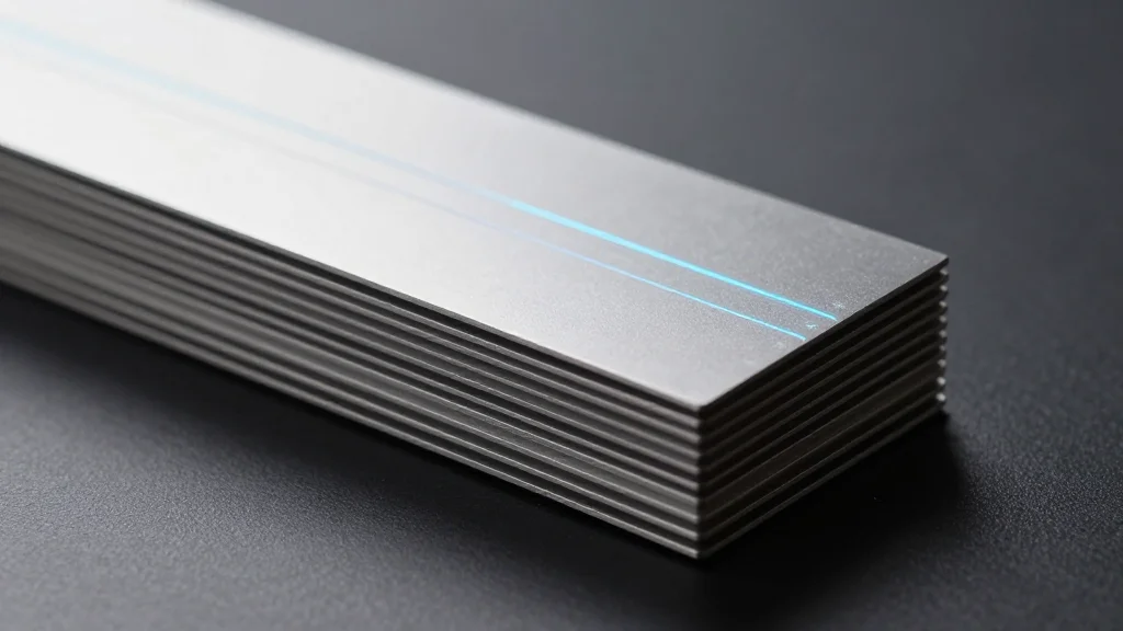
- •Samsung began shipping 12‑layer HBM4E samples to Nvidia, AMD, Google and other AI customers.
- •HBM4E offers 48 GB capacity, 30% more than HBM4, and up to 3.6 TB/s bandwidth per stack.
- •Pin speeds of 14‑16 Gbps represent a >20% performance gain over the previous generation.
- •Energy efficiency improves 16% and thermal resistance drops >14% thanks to low‑power design.
- •Samsung’s share price rose 4.34% (up to 6.5% in early trading) on the announcement.
Pulse Analysis
Samsung’s aggressive rollout of HBM4E samples is more than a product launch; it’s a strategic play to lock in design wins for the next wave of AI accelerators. By leveraging its vertically integrated stack—DRAM, logic, and advanced packaging—Samsung can promise customers a seamless path from prototype to volume, a value proposition that rivals lacking such integration (e.g., Micron) may struggle to match. The timing is crucial: AI model sizes are expanding faster than Moore’s Law can deliver transistor density, making memory bandwidth the new bottleneck. Samsung’s 3.6 TB/s per stack directly addresses that choke point, potentially enabling larger context windows and lower latency inference.
From a market‑share perspective, the sample shipments could accelerate Samsung’s recovery from a dip to 22% HBM share last quarter. If the company can sustain high yields at the 4‑nm base die and 1c DRAM node, it may erode SK Hynix’s lead, especially as Hynix’s own roadmap for HBM5 remains several quarters away. Price dynamics will also shift; with analysts forecasting a 50%+ price rise, early‑stage suppliers like Samsung can command premium pricing, improving margins in a segment traditionally squeezed by DRAM price volatility.
Looking forward, the real test will be Samsung’s ability to transition from samples to mass production without yield setbacks. The Pyeongtaek P5 fab’s capacity, the reliability of the 4‑nm logic die, and the scalability of the low‑power packaging will determine whether Samsung can meet the aggressive timelines of hyperscale cloud providers. If successful, Samsung could set a new performance baseline for AI hardware, compelling competitors to accelerate their own next‑gen HBM roadmaps and potentially reshaping the competitive landscape of AI infrastructure for years to come.
Samsung Ships First 12‑Layer HBM4E Samples, Boosting AI Memory Lead
Comments
Want to join the conversation?
Loading comments...