Scientists Built a Memory Chip that Breaks the Rules of Miniaturization
Why It Matters
The new memory architecture cuts energy consumption and heat generation, addressing a key bottleneck in mobile and edge computing. Its integration potential could spur a wave of longer‑lasting, more efficient electronic devices across multiple industries.
Key Takeaways
- •25‑nm ferroelectric tunnel junction built using hafnium oxide.
- •Device performance improves as size shrinks, defying conventional scaling limits.
- •New electrode heating method creates near‑single‑crystal structure, reducing leakage.
- •Potential to extend smartwatch battery life to months and power AI chips.
Pulse Analysis
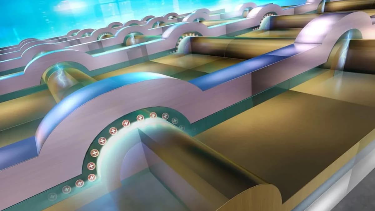
The ferroelectric tunnel junction (FTJ) has been a long‑standing candidate for ultra‑low‑power memory, but scaling below 50 nm traditionally caused polarization loss and leakage at crystal boundaries. In 2011 researchers discovered that hafnium oxide retains ferroelectricity even when only a few atomic layers thick, opening a path to extreme miniaturization. Building on that insight, Professor Yutaka Majima’s team at the Institute of Science Tokyo fabricated a 25‑nm FTJ by heating the electrodes until they formed a semicircular, near‑single‑crystal shape. This geometry dramatically cuts leakage paths, allowing the device to not only function but actually improve as it shrinks.
A memory cell that consumes orders of magnitude less energy could reshape power‑hungry electronics. Smartwatches and other wearables, which currently require daily charging, might run for months on a single battery, while dense sensor networks could operate unattended for years. In artificial‑intelligence accelerators, the ultra‑small, low‑voltage FTJ could deliver faster data access without the thermal penalties of conventional SRAM or DRAM, enabling more efficient edge‑AI processing. The reduction in heat generation also eases cooling demands in data‑center servers.
Because hafnium oxide is already a standard high‑k dielectric in CMOS manufacturing, the new FTJ can be integrated into existing fab lines with minimal retooling. Analysts estimate that, if volume production begins within the next five years, the market for low‑power non‑volatile memory could grow by double‑digit percentages annually, driven by the IoT and autonomous‑vehicle sectors. Venture capital and government research programs are already earmarking funds for ferroelectric‑based devices, suggesting that the breakthrough may quickly move from laboratory prototypes to commercial chips that redefine energy efficiency standards across the semiconductor industry.
Scientists built a memory chip that breaks the rules of miniaturization
Comments
Want to join the conversation?
Loading comments...