Stress-Tested, Future-Ready GaN
Why It Matters
Robust GaN reliability removes a critical barrier to widescale adoption, enabling higher efficiency power electronics that drive decarbonisation and performance gains across high‑growth sectors.
Key Takeaways
- •Infineon’s lateral GaN HEMTs deliver low on‑state resistance at high breakdown voltage
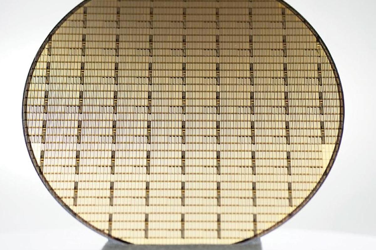
- •Wafer‑level DHTOL testing evaluates thousands of devices daily, accelerating reliability data
- •Reliability program exceeds JEDEC baseline, targeting sub‑100 FIT failure rates
- •Charge trapping and mechanical stress are primary GaN failure mechanisms
- •Wide‑bandgap adoption could cut 150 M tons CO₂ annually by 2030
Pulse Analysis
The semiconductor landscape is shifting as wide‑bandgap materials like gallium nitride (GaN) move from niche to mainstream. GaN’s wide bandgap, high critical electric field and rapid electron drift enable devices that are both smaller and more efficient than silicon equivalents. Lateral HEMT architectures exploit a two‑dimensional electron gas to achieve record low on‑resistance for a given voltage rating, making them ideal for high‑frequency chargers, solar micro‑inverters and AI‑centric data‑center power supplies. This material complementarity—silicon for low‑voltage, SiC for ultra‑high voltage, GaN for high‑frequency, high‑efficiency—creates a versatile toolkit for the electrified future.
Reliability, however, has been the Achilles’ heel of GaN power devices. Infineon tackles this by integrating accelerated high‑temperature operating life (DHTOL) tests at the wafer level, allowing thousands of devices to be stressed simultaneously. The approach captures voltage‑dependent degradation and charge‑trapping effects, feeding into physics‑based lifetime models that predict 15‑year operation at 700 V. Coupled with extensive burn‑in campaigns covering over 100,000 parts, the company can quantify infant‑mortality and wear‑out rates far below standard JEDEC FIT thresholds, delivering confidence to automotive and industrial customers.
The broader impact is substantial. As e‑mobility, AI‑driven factories and data‑center demand surge, GaN’s efficiency gains translate into lower energy consumption and reduced CO₂ emissions—potentially trimming 150 million tons of carbon annually by 2030. With proven reliability, manufacturers can design more compact, lighter power modules, accelerating time‑to‑market for next‑generation electric vehicles and high‑performance computing. Infineon’s rigorous methodology thus not only de‑risks GaN adoption but also positions the technology as a cornerstone of the global decarbonisation agenda.
Stress-tested, future-ready GaN
Comments
Want to join the conversation?
Loading comments...