Trends in Semiconductor Manufacturing: Wafer-Level and Panel-Level Packaging
Why It Matters
Advanced process technologies now dictate yield, cost and speed to market for AI, 5G and HPC chips, while sustainable manufacturing safeguards long‑term profitability and regulatory compliance.
Key Takeaways
- •WLP remains core, but process tech now defines packaging success
- •PLP scaling demands uniform plating and PECVD across large panels
- •Sustainability drives closed‑loop wet and plating systems in HVM
- •ACM Research offers front‑end‑grade tools for both wafer and panel packaging
Pulse Analysis
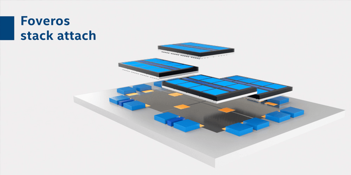
The race to integrate more functionality into smaller footprints has elevated wafer‑level packaging (WLP) from a niche to a cornerstone of advanced semiconductor manufacturing. Yet the real differentiator is no longer the package architecture alone; it is the suite of front‑end‑grade processes—wet chemistry, electrochemical plating and plasma‑enhanced CVD—that enable high‑aspect‑ratio TSVs, ultra‑fine redistribution layers and reliable chiplet bonding. As heterogeneous integration matures, these process steps must deliver sub‑micron precision and defect‑free uniformity, especially when transitioning to panel‑level packaging (PLP) where substrate sizes multiply the complexity of fluid dynamics and deposition uniformity.
Concurrently, the industry faces mounting sustainability mandates. Traditional wet and plating operations consume large volumes of chemicals and water, prompting manufacturers to adopt closed‑loop systems, real‑time chemical recycling and optimized mass‑transport designs. These innovations not only cut operating expenses but also reduce environmental footprints, aligning high‑volume manufacturing (HVM) with ESG goals. Companies that embed such eco‑efficient capabilities into their toolsets gain a competitive edge, delivering both performance and cost advantages.
Against this backdrop, ACM Research leverages its front‑end semiconductor expertise to supply packaging‑specific solutions that bridge the gap between wafer and panel production. Its electrochemical plating platforms promise void‑free fills in deep TSVs, while its wet processing suites integrate chemical‑reuse loops to lower waste. By providing tools that marry precision with sustainability, ACM positions itself as a strategic partner for OSATs and fabless firms seeking to accelerate AI, 5G and high‑performance computing roadmaps without compromising yield or environmental responsibility.
Trends in Semiconductor Manufacturing: Wafer-Level and Panel-Level Packaging
Comments
Want to join the conversation?
Loading comments...