TSMC Defends Transistor Scaling Amid Huawei’s ‘Her’s Law’ Proposal
Companies Mentioned
Why It Matters
The debate underscores whether the semiconductor industry will pivot to 3‑D density metrics or continue investing in transistor miniaturization, a decision that shapes R&D spending, equipment demand, and competitive advantage.
Key Takeaways
- •TSMC emphasizes transistor scaling as primary efficiency driver
- •Huawei's Her’s Law promotes 3‑D integration over transistor count
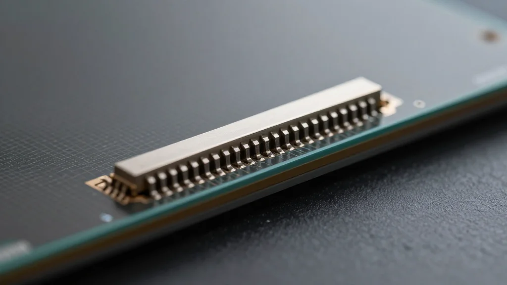
- •CFETs stack p‑ and n‑FETs, doubling density per footprint
- •TSMC’s Dresden fab aims for high‑volume production by 2029
- •Shrinking from N2 to A14 yields ~30% power reduction
Pulse Analysis
Huawei’s “Her’s Law” attempts to reframe semiconductor progress by focusing on overall speed‑up through Tao scaling, a 3‑D integration concept that sidesteps the traditional transistor‑per‑square‑millimeter metric. The proposal arrives as the industry grapples with the physical limits of extreme ultraviolet (EUV) lithography, prompting foundries like TSMC to publicly reaffirm the value of continued transistor miniaturization while acknowledging the complementary role of vertical stacking technologies.
In technical terms, 3‑D integration and stacking can boost compute density without adding more transistors to a single die, a point TSMC’s Zhang highlighted when discussing Huawei’s stacking claims. However, he stressed that transistor geometry shrinkage still offers the most dramatic efficiency gains—approximately a 30% reduction in power consumption when moving from N2 to A14 nodes—far outpacing incremental improvements such as delivering 800 V directly to data‑center racks, which only yields low‑single‑digit gains. Emerging structures like complementary‑field‑effect transistors (CFETs) exemplify how vertical stacking can double functional density within the same footprint, marrying the benefits of 3‑D design with traditional scaling.
From a business perspective, TSMC’s control of EUV equipment and its roadmap anchored in geometry reduction give it a strategic edge over competitors lacking such tools. The company’s European venture, ESMC, slated for high‑volume output by 2029, will focus on automotive and industrial chips, reinforcing TSMC’s global supply chain resilience. As customers weigh the trade‑offs between incremental 3‑D gains and the substantial power savings of continued scaling, TSMC’s stance signals that transistor innovation will remain the cornerstone of semiconductor advancement, shaping R&D budgets and market dynamics for the next decade.
TSMC Defends Transistor Scaling Amid Huawei’s ‘Her’s Law’ Proposal
Comments
Want to join the conversation?
Loading comments...