TSMC Lays Out ‘Three-Layer Cake’ Vision for AI Chips
Companies Mentioned
Why It Matters
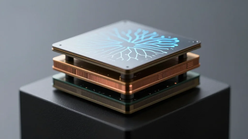
By unifying compute, packaging and photonic connectivity, TSMC positions itself to capture the bulk of AI‑driven wafer demand and lock in higher‑margin services across the entire chip stack.
Key Takeaways
- •TSMC's 2nm N2 node entered mass production Q4 2025.
- •Over 25 N2 tape‑outs received; 70 more designs in pipeline.
- •CoWoS packaging capacity to grow ~85% YoY in 2026.
- •COUPE photonic interconnects target AI data‑movement bottleneck.
Pulse Analysis
The "three‑layer cake" model reflects a shift from siloed semiconductor processes to a holistic architecture where compute, packaging and photonics are co‑designed. TSMC’s 2nm N2 node delivers the transistor density needed for next‑generation AI accelerators, while its Chip‑on‑Wafer‑on‑Substrate (CoWoS) platform stacks multiple dies into a single high‑bandwidth package. Adding COUPE’s silicon‑photonic links tackles the growing data‑movement bottleneck that traditional electrical interconnects cannot sustain, enabling terabit‑per‑second communication between dies and reducing latency for large language models.
Market analysts see AI chips driving the majority of the semiconductor boom, and TSMC’s integrated roadmap directly addresses that demand. The company’s forecast of $1 trillion in chip revenue this year—four years ahead of prior estimates—underscores the accelerating adoption of AI workloads. With AI and high‑speed computing projected to account for 55% of a $1.5 trillion market by 2030, TSMC’s ability to supply both the advanced wafers and the sophisticated packaging and photonic layers gives it a competitive moat that rivals will find hard to match without comparable vertical integration.
However, the success of this vision depends on ecosystem readiness. Customers must redesign their chip stacks to exploit CoWoS and photonic interfaces, and the supply chain for silicon‑photonic components must scale rapidly. If TSMC can align its foundry capacity, packaging lines, and photonic fabs, it will not only lock in high‑margin AI business but also set a new industry standard for integrated chip design, compelling other foundries to pursue similar multi‑layer strategies or risk losing relevance in the AI‑centric future.
TSMC Lays Out ‘Three-Layer Cake’ Vision for AI Chips
Comments
Want to join the conversation?
Loading comments...