TSMC Unfolds Map for Process, Packaging Tech
Companies Mentioned
Why It Matters
The roadmap positions TSMC to dominate the fast‑growing AI chip market while delivering lower power and latency, reinforcing its competitive edge without heavy high‑NA EUV investment.
Key Takeaways
- •A14 1.4nm GAA launches 2028 for AI data‑center chips
- •A13 reduces chip size 6% versus A14, production 2029
- •N2U 2nm derivative cuts power up to 10% starting 2028
- •COUPE photonics and larger CoWoS halve latency, improve efficiency 2.5×
- •TSMC targets >$1.5 trillion AI chip market by 2030, 55% from HPC
Pulse Analysis
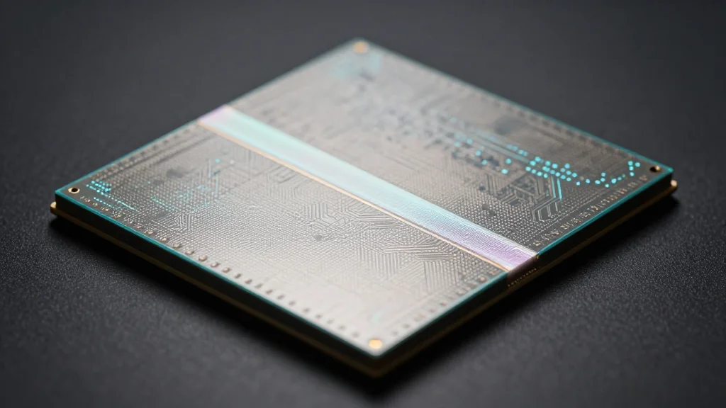
TSMC’s latest roadmap signals a strategic shift from pure lithographic scaling to a hybrid model that leverages advanced packaging and silicon photonics. By introducing the A14 1.4‑nm gate‑all‑around node and its A13/A12 successors, the foundry promises modest die‑size reductions while maintaining performance gains for AI accelerators. The N2U derivative of the 2‑nm platform adds a 10% power‑efficiency edge, a critical metric as data‑center operators grapple with rising electricity costs and sustainability targets. This approach allows TSMC to sidestep the steep capital outlay of high‑NA EUV equipment—each tool priced around $380 million—while still delivering next‑generation node capabilities.
The packaging innovations are equally transformative. TSMC’s COUPE (Compact Universal Photonics Engine) and expanded CoWoS interposers aim to bring memory and compute closer together, delivering up to a 2× latency reduction and a 2.5× boost in power efficiency. By moving toward system‑on‑wafer (SOW) architectures, the company eliminates traditional substrates, enabling wafer‑scale integration that rivals the early‑stage efforts of Cerebras. These advances not only meet the immediate demand for high‑bandwidth AI workloads but also lay the groundwork for future heterogeneous compute ecosystems.
From a market perspective, TSMC’s confidence in a $1.5 trillion AI semiconductor market by 2030 underscores the sector’s rapid expansion. With high‑performance computing projected to account for more than half of that revenue, the foundry’s ability to deliver cost‑effective, power‑efficient chips without relying on high‑NA EUV could reshape supply‑chain dynamics. Competitors like Intel, which have already adopted high‑NA tools, may face pressure to justify their higher cost structures, while smaller players eyeing silicon‑photonics see TSMC’s roadmap as a benchmark for scaling their own offerings.
TSMC Unfolds Map for Process, Packaging Tech
Comments
Want to join the conversation?
Loading comments...