Wolfspeed Unveils Foundation for AI Data-Center Advanced Packaging Leveraging 300mm Silicon Carbide
•March 10, 2026
0
Why It Matters
The new SiC platform could overcome thermal and reliability limits of current AI data‑center packages, unlocking higher performance and lower cost at scale. Its compatibility with existing 300 mm fab tools accelerates industry adoption.
Key Takeaways
- •300 mm SiC wafers ready for AI/HPC packaging.
- •High thermal conductivity tackles data‑center heat challenges.
- •Platform aligns with existing 300 mm semiconductor fabs.
- •Partners include foundries, OSATs, system architects.
- •Enables larger interposers, improving power density handling.
Pulse Analysis
The explosive growth of artificial‑intelligence models has forced data‑center designers to push silicon packages beyond traditional limits. As chip counts climb and power densities exceed 200 W/cm², conventional copper‑based interposers and organic substrates struggle with heat removal and mechanical stress. Advanced heterogeneous integration—stacking processors, memory and accelerators—exacerbates these issues, creating a bottleneck for next‑generation AI and high‑performance computing workloads. Industry analysts predict that without a breakthrough in substrate materials, scaling performance per watt will stall, prompting semiconductor leaders to explore alternatives such as wide‑bandgap semiconductors.
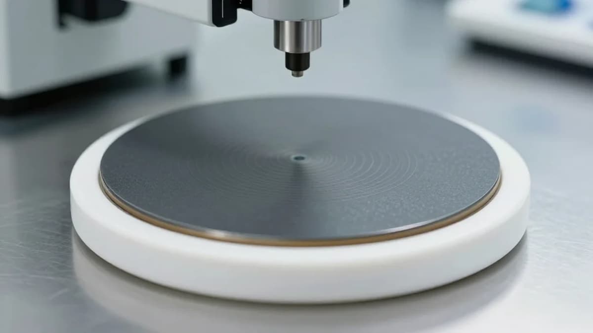
Silicon carbide, a wide‑bandgap material, offers thermal conductivity up to three times that of silicon while maintaining excellent electrical insulation. Wolfspeed’s 300 mm SiC wafer, the first single‑crystal format at this size, fits directly into the existing 300 mm fab ecosystem, allowing manufacturers to reuse lithography, deposition and etch tools without costly retooling. This alignment reduces capital expenditure and shortens time‑to‑volume for AI‑optimized packages. Moreover, the larger wafer diameter supports bigger interposers and heat‑spreader plates, enabling designers to spread heat more efficiently across densely packed die stacks.
Wolfspeed’s collaborative partner program brings together foundries, outsourced semiconductor assembly and test (OSAT) providers, system architects and research labs to validate SiC’s reliability under real‑world AI workloads. Early results suggest improved thermal cycling endurance and lower junction temperatures, translating into longer device lifetimes and reduced cooling infrastructure costs. If the industry adopts hybrid SiC‑silicon packaging at scale, data‑center operators could achieve higher compute density while curbing energy consumption, reinforcing the economic case for AI expansion. The move positions SiC as a strategic enabler in the evolving semiconductor supply chain.
Wolfspeed unveils foundation for AI data-center advanced packaging leveraging 300mm silicon carbide
0
Comments
Want to join the conversation?
Loading comments...