3D Glass Solutions Commits $234 M to Advanced Chip‑packaging Plant in Odisha
Companies Mentioned
Why It Matters
The 3DGS investment marks a decisive step toward self‑sufficiency in high‑performance semiconductor packaging for India. By introducing glass‑ceramic substrates with lower dielectric constants, the plant can deliver faster, more power‑efficient chips for AI, HPC and 5G/6G applications, reducing latency and energy consumption across critical sectors. Moreover, the vertically integrated model could lower overall cost structures, making India a more attractive destination for global fabless firms seeking to diversify away from traditional silicon‑centric supply chains. Beyond technology, the project signals a shift in Odisha’s industrial identity. Historically dependent on mining and heavy metals, the state is now courting high‑value electronics manufacturing, leveraging central subsidies and the presence of multinational investors like Intel and Lockheed Martin. If successful, the plant could catalyze a cluster effect, spurring ancillary services, talent development and export opportunities, thereby strengthening India’s position in the global semiconductor hierarchy.
Key Takeaways
- •3D Glass Solutions commits ₹1,943 crore ($234 M) to build an advanced chip‑packaging plant in Odisha.
- •Planned 2030 capacity: 69,600 glass panel substrates, 50 million assembled units, 13,200 3DHI modules per year.
- •Central government backs the project with ₹799 crore; Odisha adds ₹399.5 crore in subsidies.
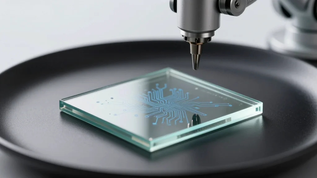
- •The facility will use 3DGS’s patented APEX glass‑ceramic technology, offering a dielectric constant of 3‑6 versus 11.7 for silicon.
- •Construction has begun; first production line expected by late 2028, pending environmental and SEZ clearances.
Pulse Analysis
3D Glass Solutions’ foray into India arrives at a moment when global chip‑packaging capacity is tightening amid geopolitical tensions and supply‑chain disruptions. By betting on glass‑ceramic substrates, 3DGS is betting on a technology that could sidestep the lithography bottlenecks that have plagued silicon fabs for years. The lower dielectric constant and superior high‑frequency performance directly address the needs of AI accelerators and 5G/6G radios, markets projected to grow at double‑digit rates through the next decade. If the panel‑level processing line scales as intended, 3DGS could set a new cost‑per‑performance benchmark, forcing traditional OSAT players to reconsider their material roadmaps.
From a policy perspective, the project underscores the effectiveness of India’s subsidy framework, which blends central and state funds to de‑risk capital‑intensive ventures. The absence of external debt at this stage suggests confidence in the equity partners and the strategic importance placed on the plant by the Indian government. However, the venture’s reliance on emerging panel technology introduces execution risk; any delay in achieving reliable 510 mm‑scale processing could erode the projected cost advantages and push back the 2030 production target.
Strategically, the Odisha plant could become a magnet for downstream fabless companies looking to source advanced packaging locally, especially those targeting defense and aerospace contracts where security and supply‑chain resilience are paramount. The involvement of Intel and Lockheed Martin as investors adds credibility and may open doors to classified programs, further differentiating the site from generic OSAT facilities. In the longer term, success here could inspire a wave of glass‑based packaging plants across emerging economies, reshaping the global semiconductor ecosystem away from a silicon‑centric paradigm toward a more diversified material landscape.
3D Glass Solutions commits $234 M to advanced chip‑packaging plant in Odisha
Comments
Want to join the conversation?
Loading comments...