
Why It Matters
Accurate, non‑destructive defect detection enables manufacturers to fine‑tune material properties, reducing waste and improving product performance. The breakthrough positions AI as a core tool for next‑generation materials engineering.
Key Takeaways
- •AI model identifies up to six point defects in semiconductors
- •Uses non‑invasive neutron scattering data for quantitative defect analysis
- •Trained on 2,000 semiconductor samples covering 56 elements
- •Detects defect concentrations as low as 0.2 percent
- •Approach could extend to Raman spectroscopy for faster industry adoption
Pulse Analysis
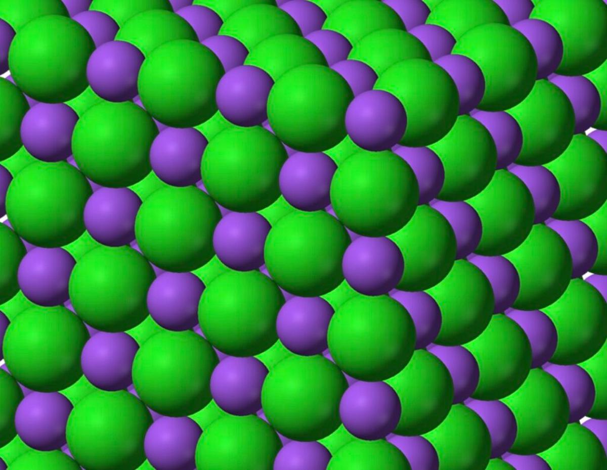
Defects have long been a double‑edged sword in materials science: they can be engineered to boost strength, conductivity, or efficiency, yet their precise measurement has remained elusive. Conventional techniques such as X‑ray diffraction, Raman spectroscopy or transmission electron microscopy each capture only a fragment of the defect landscape and often require destructive sample preparation. This limitation forces manufacturers to rely on estimates, increasing the risk of performance shortfalls in high‑value products like microchips and solar panels.
The MIT team tackled this gap by marrying neutron‑scattering spectroscopy with a multi‑head attention AI model, similar to the architecture behind ChatGPT. By feeding the model paired datasets—one pristine, one doped—for 2,000 semiconductor compounds, the system learned to isolate the subtle vibrational signatures of six distinct point defects. In validation tests, it accurately quantified defect concentrations down to 0.2 percent, a sensitivity far beyond what any single conventional method can achieve. The approach demonstrates how deep learning can decode complex, overlapping signals that would appear indistinguishable to the human eye.
For industry, the implications are profound. A reliable, non‑destructive defect sensor could streamline quality‑control pipelines, reduce scrap rates, and accelerate the rollout of next‑generation devices. While neutron facilities are not yet commonplace on production floors, the researchers are already exploring Raman‑based adaptations that could bring the technology to standard labs. As AI continues to infiltrate materials discovery, this work exemplifies a new paradigm where machine perception complements human expertise to unlock superior material performance.
A model for defect identification in materials
Comments
Want to join the conversation?
Loading comments...