AI Models Transform Defect Inspection And Review, But Can Fail To Scale
Companies Mentioned
Why It Matters
Effective AI scaling can unlock significant yield gains and cost savings across semiconductor fabs, while failure to integrate data hampers competitiveness. The shift determines which manufacturers can maintain edge in advanced packaging and node development.
Key Takeaways
- •AI boosts defect capture rate, distinguishing yield‑killing from nuisance defects
- •Deep‑learning models detect wafer‑edge defects missed by traditional inspection
- •Synthetic data and augmentation overcome scarce defect samples for training
- •Over 70% of AI pilots stall due to fragmented data, legacy systems
- •Scalable AI needs integrated data platforms, digital twins, and enterprise AI infrastructure
Pulse Analysis
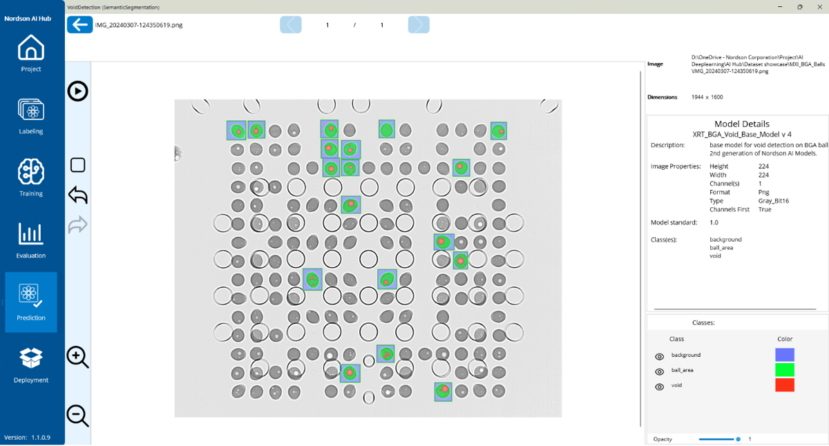
The semiconductor industry is witnessing a paradigm shift as artificial‑intelligence models become central to defect inspection. Unlike conventional statistical algorithms, deep‑learning systems excel at pattern recognition, enabling engineers to capture a broader spectrum of defect types across lithography, patterning, and advanced packaging steps. By automatically distinguishing yield‑killing defects from benign anomalies, AI drives higher capture rates and accelerates root‑cause analysis, directly translating into improved wafer yields and reduced time‑to‑market for next‑generation chips.
Despite these advantages, the transition from pilot to production remains fraught with obstacles. Over 70% of AI initiatives falter after initial trials, primarily because fragmented data silos, legacy manufacturing execution systems, and insufficient metadata undermine model reliability. Companies are turning to synthetic data generation and hybrid physics‑ML models to mitigate the scarcity of labeled defect samples, especially for emerging processes like hybrid bonding. Robust data engineering—standardized sensors, AI‑ready repositories, and seamless CIM/MES integration—is emerging as the decisive factor that separates successful scale‑ups from stalled projects.
Industry leaders now outline a structured roadmap to achieve enterprise‑wide AI adoption. Core pillars include SEMI‑compliant equipment, digital twins for factory planning, a unified knowledge hub, and multi‑agent platforms that blend autonomous decision‑making with expert feedback. When these elements converge, AI not only refines inspection accuracy but also enhances metrology, automates defect classification, and supports autonomous engineering with human oversight. For semiconductor manufacturers, mastering this data‑centric AI ecosystem is essential to sustain yield improvements, lower operational costs, and maintain a competitive edge in an increasingly complex technology landscape.
AI Models Transform Defect Inspection And Review, But Can Fail To Scale
Comments
Want to join the conversation?
Loading comments...