MIT Researchers Use AI to Uncover Atomic Defects in Materials
Why It Matters
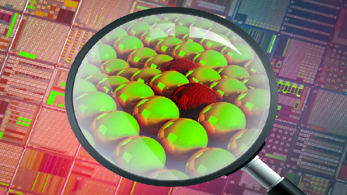
Accurate, non‑destructive defect detection enables manufacturers to fine‑tune material properties, reducing waste and improving performance of semiconductors, solar cells, and batteries. The breakthrough positions AI as a core tool for next‑generation materials engineering and could accelerate adoption of defect‑engineered products.
Key Takeaways
- •AI model classifies six point defects from neutron scattering data
- •Trained on 2,000 semiconductor samples covering 56 elements
- •Detects defect concentrations as low as 0.2 percent
- •Non‑invasive technique avoids damaging finished materials
- •Industry eyeing Raman‑based AI models for faster deployment
Pulse Analysis
The MIT study marks a turning point in materials science by marrying advanced machine‑learning architectures with neutron‑scattering spectroscopy. Traditional defect‑characterization tools—X‑ray diffraction, Raman, TEM—each capture only a slice of the defect landscape, often requiring invasive sample preparation. By leveraging a multi‑head attention model similar to those powering large language models, the researchers extracted subtle vibrational signatures that differentiate up to six defect types simultaneously. This capability not only streamlines the analytical workflow but also opens the door to real‑time monitoring of defect profiles during manufacturing.
From a commercial perspective, the ability to quantify defects without destroying the product could reshape quality‑control practices across the semiconductor, solar‑cell, and battery sectors. Current production lines rely on statistical sampling and destructive testing, which introduce latency and material loss. An AI‑driven, non‑invasive solution promises higher throughput, lower scrap rates, and tighter control over dopant concentrations—critical factors for yield optimization and cost reduction. Companies that integrate such technology may gain a competitive edge by delivering more reliable, high‑performance components.
Looking ahead, the research team’s next milestone is translating the neutron‑scattering workflow to Raman spectroscopy, a technique already entrenched in industrial labs. If successful, the AI model could be deployed on existing equipment, dramatically shortening the adoption curve. Moreover, expanding the model to recognize larger defect structures like grain boundaries could further enhance material design strategies. As AI continues to prove its pattern‑recognition prowess, its role in defect science is poised to evolve from a niche research tool to a mainstream engineering asset.
MIT Researchers Use AI to Uncover Atomic Defects in Materials
Comments
Want to join the conversation?
Loading comments...