Quantum Diamond Microscopy – Solving the Inspection Gap in Advanced Packaging
Why It Matters
QDM adds true electrical insight to the metrology toolbox, accelerating root‑cause analysis and reducing yield‑loss risk in increasingly complex packaging stacks.
Key Takeaways
- •Quantum diamond microscopy maps current flow in fully assembled packages.
- •QDM resolves buried defects that thermography and X‑ray miss.
- •Measurement takes seconds, requires no vacuum or sample preparation.
- •Roadmap targets InFab (2027) and InLine (2028) for production‑line use.
- •Early adopters include Eurofins EAG Labs in Sunnyvale, Europe, Asia.
Pulse Analysis
The semiconductor industry’s shift toward chiplet, 2.5D and 3D stacking has outpaced the capabilities of traditional inspection tools. Optical methods excel at surface analysis, while lock‑in thermography and X‑ray computed tomography each address only part of the failure‑localization problem. As package geometries become deeper and more heterogeneous, engineers need a technique that can see through layers and directly assess electrical performance without destroying the device. This gap has driven the search for a non‑destructive, depth‑penetrating electrical probe.
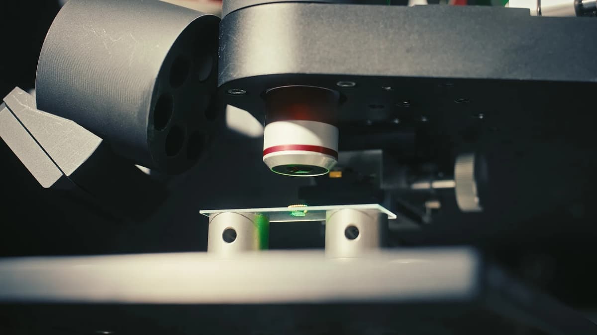
Quantum diamond microscopy leverages nitrogen‑vacancy centers in synthetic diamond to sense magnetic fields generated by current flow. When illuminated with a green laser, each NV defect shifts its quantum state in proportion to the local magnetic field, producing a wide‑field magnetic image that is mathematically reconstructed into a current‑density map. The result is a micrometer‑scale view of which interconnects, TSVs or microbumps are conducting and which are not, all captured in seconds and without vacuum chambers, cryogenic cooling, or sample alteration. Compared with thermal diffusion‑limited LIT or structurally focused X‑ray CT, QDM uniquely reveals electrically active anomalies that are invisible to other modalities.
The commercial rollout of QDM, beginning with the QDM.1 system in leading FA labs, signals a paradigm shift for both failure analysis and production metrology. Early case studies show dramatic reductions in analysis time—from days of de‑processing to a single measurement session—while preserving the device for further testing. The announced InFab (2027) and InLine (2028) configurations aim to bring this capability to lot‑level sampling and eventually 100 % in‑line inspection, promising tighter yield control and earlier defect detection. As package density and buried interconnects continue to rise, the ability to map current flow inside intact assemblies will become a critical competitive advantage for chipmakers and OEMs alike.
Quantum Diamond Microscopy – Solving the Inspection Gap in Advanced Packaging
Comments
Want to join the conversation?
Loading comments...