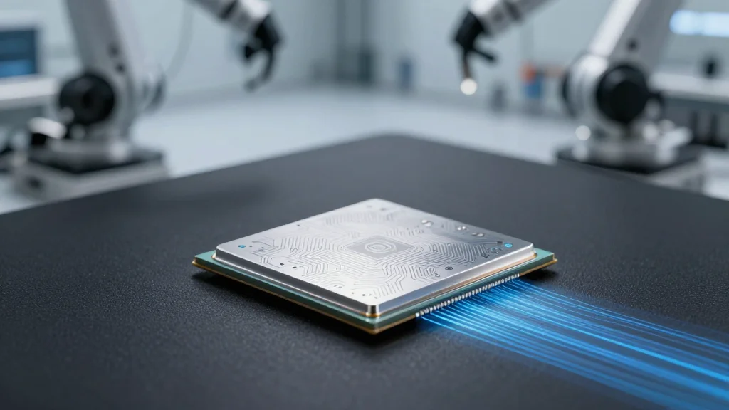
RoboSense Moves EOCENE Architecture and Dual Flagship Chips to Mass Production by 2026
Companies Mentioned
Why It Matters
The launch of mass‑production for the EOCENE architecture signals a shift toward more integrated, power‑efficient LiDAR solutions that can be embedded directly into vehicle platforms and industrial robots. By delivering a 40% reduction in silicon area and a 30% cut in power draw, RoboSense’s chips lower the cost and thermal constraints that have historically limited widespread LiDAR adoption. This could accelerate the transition from bolt‑on sensor suites to factory‑integrated perception stacks, shortening development cycles for autonomous driving and smart‑factory initiatives. Moreover, the dual‑chip strategy addresses divergent market needs: Phoenix serves high‑range, high‑resolution applications such as highway‑level autonomous driving, while Peacock caters to compact, wide‑angle sensing for blind‑spot detection and robotic vision. The ability to produce both from a common architecture simplifies supply chains and reduces engineering overhead for OEMs, potentially reshaping the competitive dynamics among LiDAR suppliers and reinforcing China’s position in the global sensor market.
Key Takeaways
- •EOCENE architecture uses a 28 nm automotive‑grade node, cutting chip area by 40% and power consumption by 30%
- •Phoenix chip processes 495 billion point‑cloud samples per second and detects objects up to 600 m
- •Peacock chip offers 640 × 480 SPAD array, millimeter‑level accuracy, and a 180° × 135° field of view
- •Both chips meet ASIL‑B functional safety standards and operate from –40 °C to 125 °C
- •Volume shipments of Peacock begin Q3 2026; Phoenix slated for mass production in 2026 after early customer trials
Pulse Analysis
RoboSense’s decision to push the EOCENE platform into mass production reflects a broader industry trend of consolidating sensor functions onto single, highly integrated silicon solutions. Historically, LiDAR systems have relied on discrete optics, lasers, and processing units, inflating cost and complexity. By embedding a 4,320‑core heterogeneous array and advanced SPAD layers on a 28 nm node, RoboSense not only achieves performance gains but also aligns with automotive manufacturers’ push for volume‑scalable, low‑power components. This mirrors the semiconductor industry’s shift from discrete to system‑on‑chip designs that has driven down costs in smartphones and data centers.
The timing is also strategic. Global LiDAR demand is projected to surge as Level‑3 and Level‑4 autonomous driving deployments accelerate, especially in China’s rapidly expanding EV market. RoboSense’s early engagement with a leading automaker for a 4‑megapixel LiDAR solution gives it a foothold that could translate into long‑term supply contracts. Meanwhile, the Peacock chip’s focus on wide‑angle, high‑density imaging opens doors beyond automotive, into logistics robots and factory automation where space constraints and sensor fusion simplicity are paramount.
Looking ahead, the success of the EOCENE rollout will hinge on RoboSense’s ability to scale manufacturing yields at the 28 nm node while maintaining ASIL‑B safety compliance. If the company can meet its Q3 2026 volume targets, it could set a new benchmark for cost‑effective, high‑performance LiDAR, forcing competitors to accelerate their own integration roadmaps or risk losing market share. The next few quarters will be a litmus test for whether integrated SPAD‑SoC designs can truly replace legacy multi‑module LiDAR stacks across the automotive and industrial sectors.
RoboSense Moves EOCENE Architecture and Dual Flagship Chips to Mass Production by 2026
Comments
Want to join the conversation?
Loading comments...