TSMC Starts Mass Production of Largest CoWoS with 98%+ Yield, Surpassing Intel and Samsung
Companies Mentioned
Why It Matters
The successful mass production of a 5.5× mask CoWoS with over 98% yield signals that TSMC can deliver the high‑density, high‑bandwidth solutions required for next‑generation AI and HPC chips. This capability reduces time‑to‑market for customers seeking to integrate more memory and logic in a single package, thereby strengthening TSMC’s value proposition in a market where performance per watt is becoming a decisive factor. For the broader manufacturing ecosystem, the announcement underscores the growing importance of advanced packaging as a lever to extend Moore’s Law beyond transistor scaling. Competitors will need to invest heavily in equipment, design tools, and supply‑chain coordination to catch up, potentially reshaping the competitive dynamics of the global foundry sector.
Key Takeaways
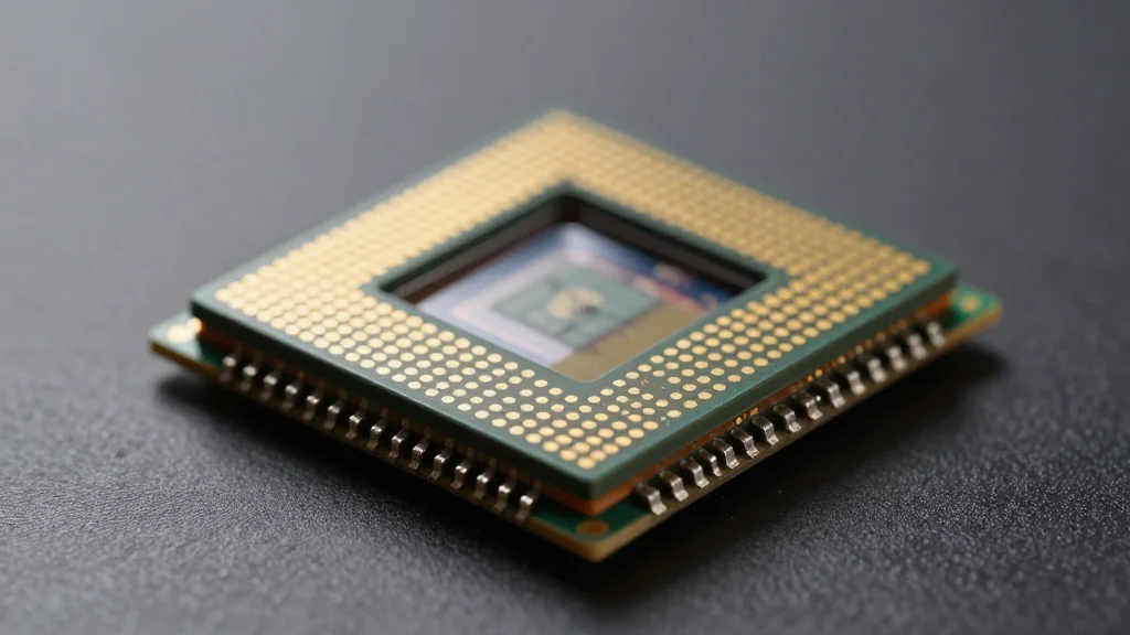
- •TSMC begins mass production of the world’s largest CoWoS (5.5× mask) with >98% yield.
- •The new package can integrate more HBM stacks, targeting AI and HPC workloads.
- •TSMC plans a 14× mask CoWoS with 20 HBM chips by 2028 and a larger version by 2029.
- •The move follows the rollout of A13, A12 and N2U process nodes slated for 2028‑2029.
- •TSMC aims for a 70% CAGR in 2nm output through 2028, reinforcing its foundry leadership.
Pulse Analysis
TSMC’s CoWoS scale‑up is more than a technical milestone; it is a strategic lever that could redefine the economics of AI chip design. By delivering a high‑yield, large‑area package, TSMC reduces the risk premium that customers traditionally assign to advanced packaging, making it a more attractive alternative to pursuing ever‑smaller process nodes. This shift aligns with the industry’s pivot toward heterogeneous integration, where performance gains are harvested by stacking memory and compute rather than shrinking transistors.
Historically, Intel and Samsung have chased lead times on wafer‑level packaging, but their public yield figures have lagged behind TSMC’s disclosed >98% benchmark. If TSMC can sustain this yield at scale, it may force rivals to accelerate their own fab upgrades or seek partnerships to bridge the gap. The ripple effect could be seen in the supply chain, from increased demand for high‑bandwidth memory suppliers to a surge in design‑tool investments for multi‑die integration.
Looking forward, the real test will be how quickly customers adopt the new CoWoS platform for production silicon. Early adopters in the AI accelerator space could lock in design wins that lock TSMC into multi‑year revenue streams, while late adopters may face higher costs or performance penalties. The upcoming 14× mask CoWoS, slated for 2028, will further stretch the envelope, potentially enabling entire GPU or TPU dies to be stacked with dozens of HBM modules. If TSMC maintains its yield advantage, the company could solidify a de‑facto standard for high‑performance packaging, shaping the competitive landscape for the next decade.
TSMC Starts Mass Production of Largest CoWoS with 98%+ Yield, Surpassing Intel and Samsung
Comments
Want to join the conversation?
Loading comments...