Gputb-2 Achieves Higher Accuracy for Electronic Structure Calculations with N^3 Scaling

Key Takeaways
- •GPUTB‑2 learns orthogonal Hamiltonians, avoiding O(N³) cost.
- •Uses E(3)-equivariant network with Gaunt and SO(2) layers.
- •Achieves 3.3 meV MAE on DeePTB, vs 19 meV prior.
- •Scales to million‑atom systems, e.g., amorphous graphene.
- •Enables accurate transport and pressure‑transition simulations.
Pulse Analysis
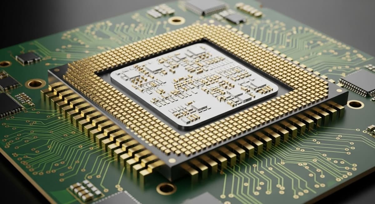
Electronic‑structure calculations based on linear combinations of atomic orbitals have long been hampered by the need to orthogonalize non‑orthogonal basis sets, a step that scales as O(N³) and quickly becomes prohibitive for large materials. Recent machine‑learning efforts aim to bypass this bottleneck, but many models require extensive parameter counts and still struggle with accuracy. GPUTB‑2 distinguishes itself by embedding orthogonality directly into the Hamiltonian learning process, eliminating the costly orthogonalization step while preserving physical symmetries.
The core of GPUTB‑2 is an E(3)-equivariant neural network that leverages a Gaunt tensor‑product layer together with an SO(2)-equivariant layer to generate both symmetric and antisymmetric tensor components of the Hamiltonian. With just 0.35 million trainable parameters, the architecture is dramatically smaller than competing approaches such as DeepH‑E3 or HamGNN, yet it delivers a mean absolute error of 3.3 meV on the DeePTB benchmark—far below the 19 meV error of its predecessor. This efficiency stems from the network’s ability to respect rotational and translational invariance, reducing the learning burden and improving generalization across diverse material systems.
The practical impact of GPUTB‑2 is evident in its application to million‑atom amorphous graphene, magic‑angle twisted bilayer graphene, and temperature‑perturbed SnSe transport studies. By offering linear‑scaling performance without sacrificing precision, the framework opens new avenues for high‑throughput materials discovery, enabling researchers to explore complex phenomena such as pressure‑induced phase transitions and large‑scale electronic transport. As the semiconductor and renewable‑energy sectors seek ever‑more sophisticated material designs, tools like GPUTB‑2 will become essential for accelerating innovation while keeping computational budgets in check.
Gputb-2 Achieves Higher Accuracy for Electronic Structure Calculations with N^3 Scaling
Comments
Want to join the conversation?