A Laser that Can Fire Light Pulses in One Billionth of a Second Is Set to Produce Structures 1000 Times Stronger, 1000 Times Faster — Novel Technique Has Applications for High-Performance Computing, Quantum Devices, and AI Chip Cooling
•January 17, 2026
0
Why It Matters
The ability to engineer heat flow at the chip‑component level enables more efficient thermal management for dense processors, improving performance and energy use in data‑center and quantum systems.
Key Takeaways
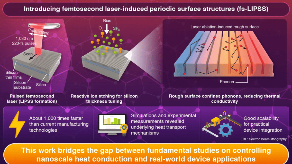
- •Femtosecond laser creates nanoscale grooves in silicon
- •Phonon scattering distance engineered to cut thermal conductivity
- •Process runs 1,000× faster than electron-beam lithography
- •Compatible with CMOS lines, maskless and resist‑free
Pulse Analysis
Traditional chip cooling relies on external heat sinks, fans, or liquid loops that remove heat only after it accumulates, limiting power density and efficiency. As processors become more compact and workloads such as AI and quantum computing demand higher performance, managing thermal transport at the material level becomes critical. By tailoring phonon pathways through nanoscale surface patterning, engineers can proactively slow heat flow where needed, offering a new lever for thermal design that complements, rather than replaces, conventional cooling methods.
The femtosecond laser‑induced periodic surface structures (fs‑LIPSS) technique uses trillionth‑of‑a‑second pulses to ablate precise grooves across silicon and silica films. This mask‑less, resist‑free process achieves nanoscale resolution while delivering throughput that exceeds electron‑beam lithography by more than three orders of magnitude, making wafer‑scale implementation feasible. Because the groove spacing aligns with phonon mean free paths, thermal conductivity drops without altering bulk material chemistry, and the resulting nanostructures exhibit mechanical strengths up to a thousand times higher than those produced by traditional etching.
For the semiconductor industry, the technology promises a paradigm shift in thermal management for high‑performance computing, quantum devices, and AI accelerators. Faster, stronger, and more controllable thermal layers could enable higher clock speeds, lower energy consumption, and denser integration of components. However, commercial adoption will hinge on reproducibility, long‑term stability, and cost‑effectiveness at data‑center scales. Ongoing collaborations between research institutes and chip manufacturers aim to validate the approach in production environments, potentially unlocking a new class of thermally optimized processors.
A laser that can fire light pulses in one billionth of a second is set to produce structures 1000 times stronger, 1000 times faster — novel technique has applications for high-performance computing, quantum devices, and AI chip cooling
0
Comments
Want to join the conversation?
Loading comments...