AI Chips Could Get Faster with 30-Nanometer Embedded Memory that Cuts Data Shuttling
Why It Matters
Embedding memory at the nanoscale eliminates the von Neumann bottleneck, boosting AI chip speed while slashing power consumption—critical for data‑center efficiency and emerging edge devices.
Key Takeaways
- •30 nm logic‑embedded memory reduces data shuttling distance.
- •Aluminum scandium nitride retains data without power, tolerates high temps.
- •Heat‑treated platinum electrodes enable 5 nm thickness without performance loss.
- •Compatible with existing semiconductor fabs, promising faster, lower‑energy AI chips.
Pulse Analysis
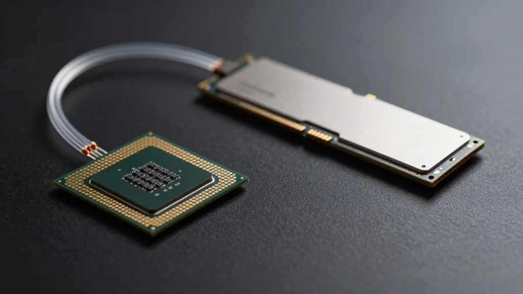
The persistent performance gap between processing units and memory—often called the von Neumann bottleneck—has become a primary obstacle for AI workloads that shuffle terabytes of data per second. Traditional architectures force data to travel between separate compute cores and DRAM banks, incurring latency and energy penalties. Logic‑embedded memory, where storage sits directly beside transistors, promises to collapse this distance, enabling on‑chip data reuse and reducing the need for costly off‑chip transfers. Materials like aluminum scandium nitride (AlScN) are especially attractive because they retain information without power (non‑volatile) and survive the high‑temperature steps of semiconductor fabrication.
In a recent study published in Advanced Electronic Materials, Professor Hiroshi Funakubo’s team engineered a full memory stack only 30 nm thick—roughly one‑three‑thousandth the width of a human hair. The breakthrough hinged on pre‑heating the platinum lower electrode, which aligned the AlScN crystal lattice and prevented the degradation typically seen in ultra‑thin films. Remarkably, the researchers also thinned the platinum electrodes to 5 nm without sacrificing endurance or switching speed, demonstrating that aggressive scaling does not inevitably compromise functionality. Electrical testing confirmed that the sub‑30 nm devices retain the same retention time and write energy as their bulkier counterparts.
The implications extend far beyond academic curiosity. Data‑center operators could see up to 30% reductions in energy use per inference task, while edge devices—from autonomous drones to smart sensors—gain the computational headroom needed for real‑time AI without draining batteries. Because the process leverages standard CMOS back‑end steps, chipmakers can adopt the technology without retooling fab lines, accelerating time‑to‑market. As AI models grow larger and latency becomes a competitive differentiator, logic‑embedded memory at the 30‑nm scale positions the semiconductor industry to deliver the next generation of high‑performance, low‑power processors.
AI chips could get faster with 30-nanometer embedded memory that cuts data shuttling
Comments
Want to join the conversation?
Loading comments...